Aldec Introduces Hardware Assisted RTL Simulation Acceleration for Microchip FPGA Designs
The latest release of HES-DVM™ provides a simulation acceleration flow, providing significant RTL simulation speed-up of designs targeting Microchip FPGA devices.
Henderson, NV, USA – November 3, 2020 – Aldec, Inc., a pioneer in mixed-HDL language simulation and hardware-assisted verification for ASIC and FPGA designs, has introduced a HES-DVM™ simulation acceleration flow for Microchip’s Polarfire, SmartFusion2 and RTSX/RTAX FPGA designs using Aldec’s HES-MPF500-M2S150 prototyping board.
“Aldec has a long history of developing hardware assisted verification solutions, with our first HES board and simulation acceleration platform released 20 years ago,” said Zibi Zalewski, General Manager of Aldec’s Hardware Division. “We also have a proven track record of developing Microsemi/Microchip FPGA prototyping boards, and it is great that we can combine these areas of expertise to meet today’s verification challenges.”
Simulation acceleration techniques have been around for about two decades, but most products are based on FPGAs from one or two leading FPGA vendors. Usually, it does not matter which FPGA family is used on the simulation acceleration board if the design is coded using synthesizable RTL.
However, growing design complexity, along with shrinking design cycles and shorter time to market, are increasingly taking engineers down the path of re-usable IP blocks from the FPGA vendor, instead of developing RTL code. The drawback is that the designs become dependent on the given FPGA technology, and the re-usable IP blocks usually require far more computational power to simulate than pure RTL code.
Aldec’s HES-DVM overcomes the above challenges and removes a key verification bottleneck. With the latest release of this powerful EDA tool, users of PolarFire, RTAX/RTSX and SmartFusion2 devices wishing to take advantage of Microchip IPs can accelerate their RTL simulations using Aldec’s HES-MPF500-M2S150, which features the largest devices available in both families.

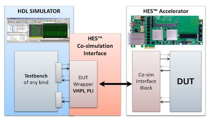
Figure 1: RTL Simulation Acceleration for Microchip FPGAs
Zalewski concludes: “During the 20 years since we introduced HES, the world of digital designs has changed significantly and the need for simulation speeds to increase has grown along with not only design complexity but also the size and features of FPGAs. Our latest release of HES-DVM will be of great benefit to designers using Microchip IPs.”
The 2020.09 software release of HES-DVM is available immediately.
About HES™ Prototyping
Aldec offers a portfolio of HES™ prototyping boards based on the largest Xilinx FPGAs of the Virtex UltraScale Plus, UltraScale and Virtex-7 families, Microsemi PolarFire and SmartFusion2. The boards are architected to allow for easy expansion using BPX backplane and standardized FMC and BPX daughter card connectors.
About HES-DVM™
HES-DVM™ is a fully automated and scalable hybrid verification environment for SoC and ASIC designs. Utilizing the latest co-emulation standards like SCE-MI or TLM and the newest FPGA technology, hardware and software design teams obtain early access to the hardware prototype of the design. HES-DVM is used in labs worldwide for all kinds of emulation and physical prototyping tasks including Simulation Acceleration, Hybrid Virtual Prototypes, In-Circuit Emulation, Software Validation and Prototyping.
About Aldec
Established in 1984, Aldec is an industry leader in Electronic Design Verification and offers a patented technology suite including: RTL Design, RTL Simulators, Hardware-Assisted Verification, SoC and ASIC Prototyping, Design Rule Checking, CDC Verification, IP Cores, High-Performance Computing Platforms, Embedded Development Systems, Requirements Lifecycle Management, DO-254 Functional Verification and Military/Aerospace solutions. www.aldec.com
Related Semiconductor IP
- ASIL B Compliant MIPI CSI-2 CSE2 Security Module
- SHA-256 Secure Hash Algorithm IP Core
- EdDSA Curve25519 signature generation engine
- DeWarp IP
- 6-bit, 12 GSPS Flash ADC - GlobalFoundries 22nm
Related News
- Aldec and Agilent Technologies Bridge the Gap Between ESL and RTL by Linking Simulation Environments
- Aldec unveils Xilinx UltraScale FPGA-based prototyping board enabling Simulation Acceleration and Emulation with the latest release of HES-DVM
- Aldec Releases Automated Static Linting and CDC Analysis for Microchip FPGA and SoC FPGA Designs
- Aldec Releases Riviera 2005.04 with All New System-Level Simulation Performance and Debugging
Latest News
- Analog Bits Demonstrates Real-Time On-Chip Power Sensing and Delivery on TSMC N2P Process at TSMC 2026 Technology Symposiums
- TES offers a High-Frequency Synthesizer and Clock Generator IP for X-FAB XT018 - 0.18µm BCD-on-SOI technology
- Faraday Delivers IP Solutions to Enable Endpoint AI Based on UMC’s 28nm SST eFlash
- AiM Future Partners with Metsakuur Company to Commercialize NPU-Integrated Hardware
- ESD Alliance Reports Electronic System Design Industry Posts $5.5 Billion in Revenue in Q4 2025