PCIe Gen 6 IP
Filter
Compare
30
IP
from
11
vendors
(1
-
10)
-
PCIe Gen 6 Phy
- Architecture optimized for HPC, AI/ML, storage, and networking
- Ultra-long reach, low latency, and low power
- Advanced DSP delivers unmatched performance and reliability
- PCIe Gen 6 Phy IPPCIe Gen 6 Phy IPComprehensive real-time diagnostic, monitor, and test features
-
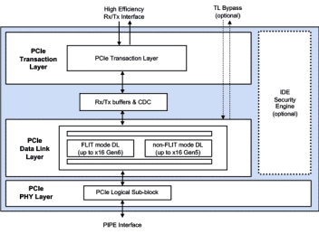
PCIe Gen 6 controller IP
- Designed to the latest PCI Express 6.0 (64 GT/s), 5.0 (32 GT/s), 4.0 (16 GT/s), 3.1/3.0 (8 GT/s), and PIPE 6.x (8, 16, 32, 64 and 128-bit) specifications
- Supports SerDes Architecture PIPE 10b/20b/40b/80b width
- Supports original PIPE 8b/16b/32b/64b/128b width
-
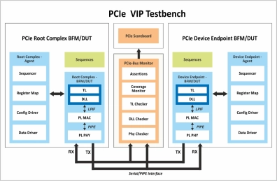
PCIe Gen 6 Verification IP
- Compliant with PCI Express Specifications 6.1 (64GT/s), 5.0 (32GT/s), 4.0 (16GT/s), 3.1 (8GT/s), 2.0 (5GT/s) and 1.1 (2.5GT/s).
- Support for 64.0 GT/s Data Rate per lane with backwards compatible.
- Support for new PAM4 Signalling and Gray Coding.
- Support for both Flit Mode & Non-Flit Mode.
-
PCIe Gen 5 Verification IP
- Support for 32.0 GT/s Data Rate per lane with backwards compatible.
- Optimizing the Link to skip equalization at lower Data Rates when supporting 32.0 GT/s(optional feature).
- Lower pin count in pipe interface when supporting 32.0 GT/s.
- Support for newly added phy serdes architecture in pipe specification 5.0 .
-
PCIe Gen 7 Verification IP
- The PCIe Gen 7 Verification IP provides an effective & efficient way to verify the components interfacing with PCIe Gen 7 interface of an IP or SoC.
- The PCIe Gen 7 VIP is fully compliant with latest PCI Express Gen 7 specifications. This VIP is a light weight with an easy plug-and-play interface so that there is no hit on the design cycle time.
-
PCIe Gen 2 Verification IP
- Compliant with PCI Express Specifications 2.0 (5GT/s) and 1.1 (2.5GT/s).
- Verification IP configurable as PCI express Root Complex and Device Endpoint.
- Configurable LinkWidth: x1, x2, x4, x8, x12, x16, x32.
- Configurable pipe width : 8,16,32,64
-
AXI PCI Express (PCIe) Gen 3
- Maximum Payload Size (MPS) up to 256 Bytes
- Messaged Signaled Interrupt (MSI)
- Memory mapped AXI4 access to PCIe space
- PCIe access to memory mapped AXI4 space
-
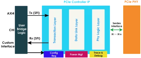
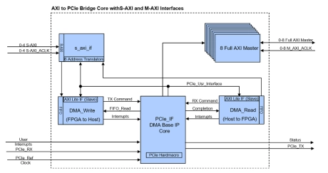
AXI Bridge for PCIe IP Core
- The AXI Bridge for PCIe IP core is the IP solution with a powerful mix of multiple industry standard memory mapped AXI Interfaces.
- The AXI Bridge IP core translates the AXI4 memory read or writes to PCI-Express Transaction Layer Packets and translates PCIe memory read and write requests to AXI4 transactions.
- All interfaces support fully parallel operation without any interferences. Interfaces that are not required can be turned off individually and do not occupy logic resources.
-
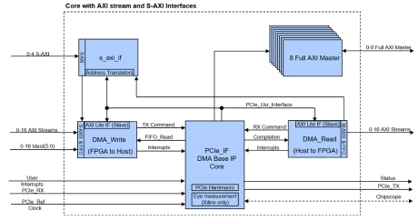
AXI Bridge with DMA for PCIe IP Core
- The AXI Bridge with DMA IP core is the ultimate PCIe DMA IP solution with a powerful mix of multiple industry standard AXI Interfaces.
- AXI Stream interfaces allow continuous data streaming from FPGA to Host or from Host to FPGA. S-AXI Memory mapped interfaces allow easy data access of remote memories in order to realize shared memory access or per to peer applications.
-