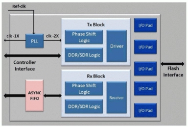
ONFI 3.0 PHY IP
Filter
Compare
5
IP
from
3
vendors
(1
-
5)
-
ONFI 3.0 Compatible I/O Buffer on TSMC CLN28HPL
- High speed, source synchronous, bi-directional I/O buffer supporting the Open NAND Flash Interface (ONFI) 3.0 standard
- Operation up to 200MHz DDR (400Mbps) performance with single load topology
- Designed with core and 1.8V IO oxide devices
- Built-in ODT (On-Die Termination)
-
ONFI 3.2 NAND Flash PHY IP Compliant to JEDEC
- Compliant to ONFI revision 3.2 standard
- Silicon proven PLL to support all frequencies from 10MHz to 266MHz, and DLL to improve data sampling accuracy dynamically
- Include ONFI 3.2 I/O pads compatible to 1.8v NV-DDR2 533 MT/s and 3v NV-DDR 200 MT/s
- Supports NV-DDR2 mode of operation supporting up to 266MHz

-
ONFI 3.2 NAND Flash Controller IP Compliant to JEDEC
- Compliant to ONFI 3.2 Specification
- Supports SDR, NV-DDR and NV-DDR2
- Included synthesizable PLL/DLL
- ONFI 3.2 compatible 1.8v NV-DDR2 I/O pads supporting up to 533MT/s is available

-
ONFI IO Pad Set
- ONFI Single-Ended Driver / Receiver Features:
- ? Driver – user-selectable on-die termination and programmable drive strength with ODT / ZO calibration and programmable “off” state control.
- o ODT Rtt = 30? / 50? / 75? / 100? / 150?
- o ZOUT = 18? / 25? / 35? / 50?
-
ONFI_4 IO Pad Set
- ONFI Single-Ended Driver / Receiver Features:
- ? Driver – user-selectable on-die termination and programmable drive strength with ODT / ZO calibration and programmable “off” state control.
- o ODT Rtt = 30? / 50? / 75? / 100? / 150?
- o ZOUT = 18? / 25? / 35? / 50?