NAND flash controller IP
Filter
Compare
47
IP
from
23
vendors
(1
-
10)
-
ONFI 3.2 NAND Flash Controller IP Compliant to JEDEC
- Compliant to ONFI 3.2 Specification
- Supports SDR, NV-DDR and NV-DDR2
- Included synthesizable PLL/DLL
- ONFI 3.2 compatible 1.8v NV-DDR2 I/O pads supporting up to 533MT/s is available

-
ONFI 2 NAND Flash Controller IP Compliant to JEDEC
- The ONFI 2.3 NAND Flash Controller IP Core is a full-featured, easy to use, synthesizable core, easily integrated into any SoC or FPGA development.
- Designed to support both SLC and MLC flash memories, ONFI 2.3 NAND controller IP is flexible in use and easy in implementation.

-
ONFI 5.0 NAND Flash Controller IP Compliant to JEDEC
- The NAND flash controller IP provides easy, reliable access to an off-chip NAND flash. It supports all modes of the Open NAND Flash Interface (ONFI) Specification, revision 5.0, release candidate 0.5, dated 1 March 2021.
- It is backwards compatible, supporting the Single Data Rate (asynchronous) mode, the double data rate moves NV-DDR, NV-DDR2, and NVDDR3, to include the latest NV-LPDDR4 recently introduced in the latest revision.

-
ONFI 4.2 NAND Flash Controller & PHY IP Compliant to JEDEC
- The NAND Flash Controller IP Core is a full-featured, easy to use, synthesizable core, easily integrated into any SoC or FPGA development.
- Designed to support SLC, MLC and TLC flash memories, it is flexible in use and easy in implementation. The controller works with any suitable NAND Flash memory device up to 1024Gb from leading memory providers – Micron, Samsung, Toshiba and Hynix.
-
NAND Flash Controller - Ensures robust NAND Flash interface validation for reliable designs
- The NAND Flash Controller Verification IP (VIP) is a specialized tool for validating and simulating NAND Flash memory interfaces in System-on-Chip (SoC) designs. It ensures compliance with protocols, error correction, and optimal performance across varied conditions.
- This versatile tool supports a wide range of applications, including automotive, consumer electronics, industrial automation, and aerospace. By guaranteeing reliable integration of NAND Flash memory, it enables seamless functionality in devices ranging from gaming consoles to mission-critical systems
-
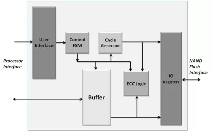
NAND Flash Controller
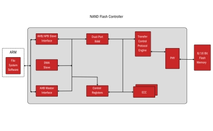
- The NFC IP is a NAND Flash Controller for accessing user data from NAND Flash chips.
- It is designed with scalability in mind and provides standard AXI interface for the ease of integration in SoC design.
- The NFC has many configurable features to support the requirements for different NAND Flash applications.
-
Nand Flash Controller
- Simple streaming interface towards user logic for data read and write
- Commands supported towards NAND Flash Memory:
- ECC Logic: Hamming code used to correct 1-bit error and detect 2-bit errors
- Commands supported from user: Block Erase, Read, Program and Copy-Back Program
-
NAND Flash Controller
- Highly Integrated IP Offering
- Speeds system integration and reduces design cost
- Command and Data DMA
- Reduces software overhead
- Wide Support of Standards
- Enables system flexibility
-
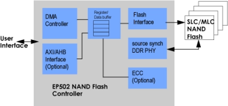
Synchronous ONFI NAND Flash Controller
- Supports single-level and multi-level cells (SLC and MLC) NAND Flash devices.
- Compatible with ONFI 2.1 Flash Interface for synchronous and asynchronous access.
- Supports source synchronous double data rate data transfer for highest possible data bandwidth.
- Supports 2k and 4k page sizes.