NAND ONFI Controller IP
Filter
Compare
27
IP
from
15
vendors
(1
-
10)
-
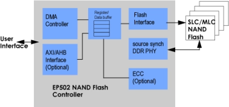
Synchronous ONFI NAND Flash Controller
- Supports single-level and multi-level cells (SLC and MLC) NAND Flash devices.
- Compatible with ONFI 2.1 Flash Interface for synchronous and asynchronous access.
- Supports source synchronous double data rate data transfer for highest possible data bandwidth.
- Supports 2k and 4k page sizes.
-
ONFI 3.2 NAND Flash Controller IP Compliant to JEDEC
- Compliant to ONFI 3.2 Specification
- Supports SDR, NV-DDR and NV-DDR2
- Included synthesizable PLL/DLL
- ONFI 3.2 compatible 1.8v NV-DDR2 I/O pads supporting up to 533MT/s is available

-
ONFI 2 NAND Flash Controller IP Compliant to JEDEC
- The ONFI 2.3 NAND Flash Controller IP Core is a full-featured, easy to use, synthesizable core, easily integrated into any SoC or FPGA development.
- Designed to support both SLC and MLC flash memories, ONFI 2.3 NAND controller IP is flexible in use and easy in implementation.

-
ONFI 5.0 NAND Flash Controller IP Compliant to JEDEC
- The NAND flash controller IP provides easy, reliable access to an off-chip NAND flash. It supports all modes of the Open NAND Flash Interface (ONFI) Specification, revision 5.0, release candidate 0.5, dated 1 March 2021.
- It is backwards compatible, supporting the Single Data Rate (asynchronous) mode, the double data rate moves NV-DDR, NV-DDR2, and NVDDR3, to include the latest NV-LPDDR4 recently introduced in the latest revision.

-
ONFI 4.2 NAND Flash Controller & PHY IP Compliant to JEDEC
- The NAND Flash Controller IP Core is a full-featured, easy to use, synthesizable core, easily integrated into any SoC or FPGA development.
- Designed to support SLC, MLC and TLC flash memories, it is flexible in use and easy in implementation. The controller works with any suitable NAND Flash memory device up to 1024Gb from leading memory providers – Micron, Samsung, Toshiba and Hynix.
-
ONFI Nand Flash Software Driver
- Compliant with ONFI 3.2 and backward compatible to ONFI 3.0, 2.3 and 1.0
- Supports SDR, NV-DDR and NV-DDR2, Toggle DDR/DDR2 modes
- Easy-to-use interface for applications
- Support up to NAND with 16K page size

-
ONFI 3.2 NAND Flash PHY IP Compliant to JEDEC
- Compliant to ONFI revision 3.2 standard
- Silicon proven PLL to support all frequencies from 10MHz to 266MHz, and DLL to improve data sampling accuracy dynamically
- Include ONFI 3.2 I/O pads compatible to 1.8v NV-DDR2 533 MT/s and 3v NV-DDR 200 MT/s
- Supports NV-DDR2 mode of operation supporting up to 266MHz
-
ONFI 5.0 NAND Fash PHY IP Compliant to JEDEC
- The ONFI 5.0 PHY IP is designed to connect seamlessly with their ONFI 5.0 Host Controller IP.
- The ONFI 5.0 PHY has complete SDR, NV-DDR, NV-DDR2, NV-DDR3 and NV-LPDDR4 TX/RX functionality and supports all the speeds defined in the ONFI specification while remaining backwards compatible with the prior versions of the ONFI specifications.
-
ONFI 4.2 NAND Flash Software Driver
- The NAND Flash Controller IP Core is a full-featured, easy to use, synthesizable core, easily integrated into any SoC or FPGA development. Designed to support SLC, MLC and TLC flash memories, it is flexible in use and easy in implementation.
- The controller works with any suitable NAND Flash memory device up to 1024Gb from leading memory providers – Micron, Samsung, Toshiba and Hynix.

-
NAND Memory Controller
- The NAND memory controller IP core is compliant with the ONFI standard working on asynchronous mode.
- This core also supports error correction on the fly without any processor intervention. Up to 8 memory chips can be accessed on the same bus with write speed of 100Mbps and read speeds of 120Mbps.