DVI IP
Filter
Compare
63
IP
from
17
vendors
(1
-
10)
-
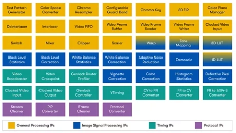
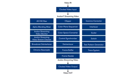
Video and Vision Processing Suite
- The Intel® FPGA Video and Vision Processing Suite is a collection of next-generation Intel® FPGA intellectual property (IP) functions that you can use to facilitate the development of custom video and image processing designs
- These Intel® FPGA IP functions are suitable for use in a wide variety of image processing and display applications, such as studio broadcast, video conferencing, AV networking, medical imaging, industrial inspections and robotics, smart city/retail and consumer.
-
Video and Image Processing Suite
- The Intel FPGA Video and Image Processing Suite is a collection of Intel FPGA intellectual property (IP) functions that you can use to facilitate the development of custom video and image processing designs
- These Intel FPGA IP functions are suitable for use in a wide variety of image processing and display applications, such as studio broadcast, video conferencing, AV networking, medical imaging, smart city/retail, and consumer.
-
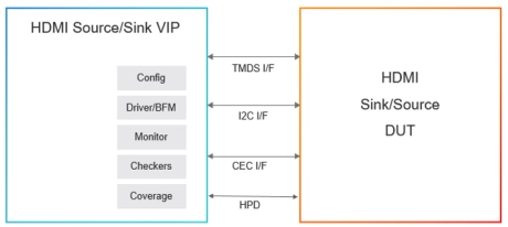
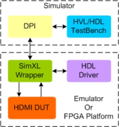
Simulation VIP for HDMI
- 3D – Capability
- Supports various 3D video frame formats
- 4K x 2K Resolution
- Supports 4Kx2K video frame formats
-
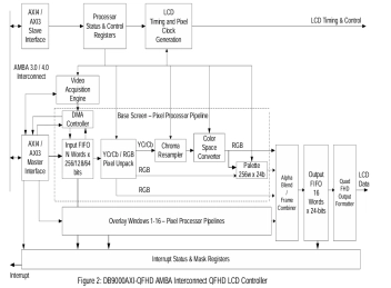
Display Controller – Ultra HD LCD / OLED Panels (AXI4/AXI Bus)
- The DB9000AXI4-UHD LCD Controller IP Core interfaces a video image in frame buffer memory via the AMBA 3.0 / 4.0 AXI Protocol Interconnect to an 4K/8K TFT LCD / OLED display panel.
- The video image in frame buffer memory can be 8/10/12-bit 4:2:0 or 4:2:2 or 4:4:4 sampled YCrCb video or 4:4:4 RGB. For 4:2:0 and 4:2:2 YCrCb, the chroma components are re-sampled to 4:4:4 and color converted to RGB.
-
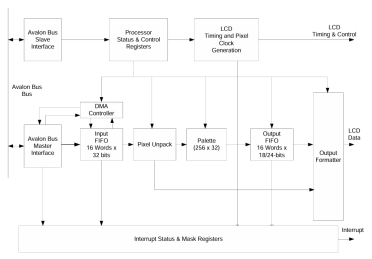
Display Controller – LCD / OLED Panels (Avalon Bus)
- The DB9000AVLN TFT LCD Controller IP Core interfaces a microprocessor and frame buffer memory via the Avalon Bus within Altera Qsys Integration (generating the System Interconnect Fabric) to a TFT LCD panel.
- In an Altera FPGA, typically, the microprocessor is a NIOS II or ARM processor and frame buffer memory is either on-chip SRAM memory or larger off-chip SRAM or SDRAM.
-
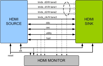
HDMI 1.4/2.0/2.1 Verification IP
- Protocol Checker fully compliant with HDMI Specification 1.4b, 2.0b and 2.1 compliant.
- Full HDMI source and sink device functionality
- Supports Video data coding.
- Supports TERC4 coding and Control period codings.
-
HDMI 1.4/2.0/2.1 Synthesizable Transactor
- Protocol Checker fully compliant with HDMI Specification 1.4b,2.0b and 2.1 compliant.
- Full HDMI source and sink device functionality
- Supports Video data coding.
- Supports TERC4 coding and Control period codings.
-
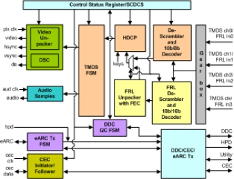
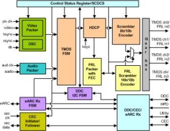
HDMI SOURCE IIP
- Compliant with HDMI specification 1.4b/2.0b/2.1.
- Full HDMI Source functionality.
- Compatible with DVI and Dual-Link DVI Standards.
- Supports 8, 10, 12 and 16 bit pixel inputs.
-
HDMI SINK IIP
- Compliant with HDMI specification 1.4b/2.0b/2.1.
- Full HDMI Sink functionality.
- Compatible with DVI and Dual-Link DVI Standards.
- Supports 8, 10, 12 and 16 bit pixel output.