DDR3 Memory Controller IP
Filter
Compare
105
IP
from
21
vendors
(1
-
10)
-
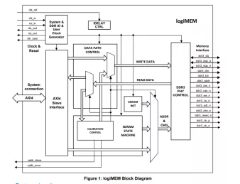
DDR3 SDRAM Memory Controller
- Supports DDR3 SDRAM memory devices on AMD-Xilinx 7 Series FPGAs
- Size optimized – ideal for low cost 7 Series FPGAs (Artix-7, Spartan-7)
-
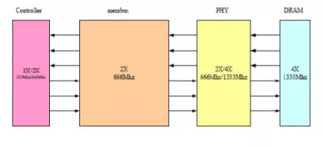
DDR 4/3 Memory Controller IP - 2400MHz
- Support s DDR 4 /DDR3 SDRAM
- 16 bit s width , Single Channel DDR 4 /DDR3 SDRAM Interface .
- 16 bits for per channel, could support 2 x8 bits DDR3, but could not support 2 x8 bits DDR4.
- Memory Clock up to 6 66 MHz, DFI Clock up to 666 MHz .
-
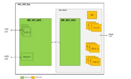
DDR4 / DDR3/ DDR3L / LPDDR4 Memory Controller IP optimized for low latency
- Support DDR3 / DDR3L / DDR4/ 3DS DDR4/ LPDDR4 / MRAM
- Support x8/x16/x32 DRAM data bus configuration (programmable)
- Support Multi-Ranks DRAM configuration
- DDR base on DFI spec 4.0 compliant.
-
High Performance DDR 3/2 Memory Controller IP
- Supports DDR3/DDR2 SDRAM
- 16 bits width DDR2/DDR3 SDRAM Interface
- Memory Clock up to 462MHz, DFI Clock up to 462MHz
- Support DDR2 667/800/1066 and DDR3 667/800/1066/1333/1600/1866
-
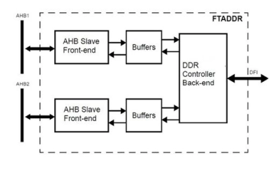
Fault Tolerant DDR2/DDR3/DDR4 Memory controller
- FTADDR is a memory controller for DDR2,DDR3 and DDR4 SDRAM memory devices.
- It uses a strong error correction code to achieve exceptional fault tolerance
-
High-Performance Memory Controller II SDRAM Intel® FPGA IP Core
- The High-Performance Memory Controller II SDRAM Intel FPGA IP core handles the complex aspects of using DDR, DDR2, and DDR3 SDRAM at speeds up to 933 MHz
- The intellectual property (IP) core initializes the memory devices, manages SDRAM banks, translates read-and-write requests from the local interface into all the necessary SDRAM command signals, and performs command and data reordering.

-
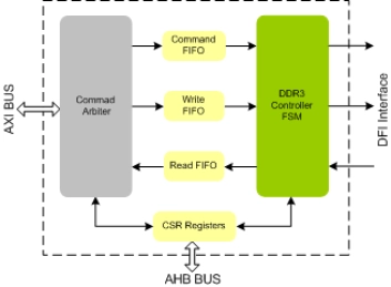
DDR3 Controller IIP
- Supports DDR3 protocol standard JESD79-3F Specification.
- Compliant with DFI-version 2.0 or higher Specification.
- Supports all the DDR3 commands as per the specs.
- Supports up to 16 AXI ports with data width upto 512 bits.
-
DDR3 SDRAM Controller IP with advance feautures package
- Supports DDR3 protocol standard JESD79-3F Specification.
- Compliant with DFI-version 2.0 or higher Specification.
- Supports all the DDR3 commands as per the specs. Supports up to 16 AXI ports with data width upto 512 bits.
- Supports controllable outstanding transactions for AXI write and read channels
-
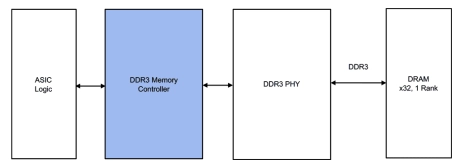
DDR3 Controller
- Maximizes bus efficiency via look-ahead command processing, bank management, auto-precharge and additive latency support
- Latency minimized via parameterized pipelining
- Achieves high clock rates with minimal routing constraints
- Supports full-rate and half-rate clock operation
- Multi-mode controller support
-
DDR3 Controller
- Component support for interface width of 8 to 80 bits (RDIMM, UDIMM, and SODIMM support)
- Controler / Phy mode or Phy only mode, plus Ping Pong Phy option
- DDR3 (1.5V)
- DDR3L (1.35V)