Other for TSMC

Welcome to the ultimate Other for TSMC hub! Explore our vast directory of Other for TSMC
All offers in Other for TSMC
Filter
Filter

Login required.

Sign in

Compare 8 Other for TSMC from 3 vendors (1 - 8)
  • Over-voltage Protection Module to handle Over-voltage operation (up to 5.5 V) while using standard process 3.3 V devices
    • Over-voltage protection biasing for embedded regulators
    • Avoids expensive solutions while enabling direct baterry connection.
    • Built-in over-voltage protection (up to 5.5 V) using 3.3 V transistors
    • Over-voltage power range: 1.9 V to 5.5 V
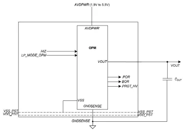
    Block Diagram -- Over-voltage Protection Module to handle Over-voltage operation (up to 5.5 V) while using standard process 3.3 V devices
  • PUF
    • Root of trust, unclonable, chip dependent ID with unique static and dynamic signature behavior in each chip
    • Process dependent, fully invisible, root of trust
    • Support 0.18um, 0.13um, 55nm, 40nm, 28nm, 14nm
    • Small Area: 0.02mm2 (140um x 140um) @SMIC 55nm
  • DP/eDP1.4/1.2 TX PHY&controller
    • Area: 0.75mm2 with pixel PLL and 0.63mm2 without pixel PLL including IO and ESD
    • Compliant with DP1.4 and eDP1.4specification
    • Typical 27MHz reference clock
    • Supports 1/2/4-lane configuration
  • DP1.4 TX PHY
    • Area: 0.75mm2 with pixel PLL and 0.63mm2 without pixel PLL including IO and ESD
    • Compliant with DP1.4 and eDP1.4specification
    • Typical 27MHz reference clock
    • Supports 1/2/4-lane configuration
  • DP/eDP1.4/1.2 RX PHY
    • Compliant with DP1.4 and eDP1.4 specifications
    • Supports 1/2/4-lane configuration
    • Up to 8.1Gbps per data lane
    • Typical 24MHz or 27MHz reference clock
  • HSIC PHY
    • Consumes <90mW during data transfer
    • Consumes <50uW when not transferring data
    • Uses standard chip digital and IO supplies
    • Low pin count
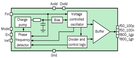
  • 800/1000 MHz DLL-based frequency multiplier
    • TSMC 90 nm CMOS
    • Low jitter
    • Precisely aligns the clock distribution output with a reference clock
    • Low current consumption
  • Over-voltage Protection Module
    • Implement power networks supporting up to 5.5 V&#8203;
    • High voltage protection (> 1.98 V) for LDO & DC/DC&#8203;
    • Low BoM Cost: no output capacitor, no extra pin&#8203;
    • Generation of low power biasing currents and voltages&#8203;
×
Semiconductor IP