Aldec 推出 HES-DVM 原型“云版”—让设计工程师更轻松地访问基于 FPGA 的 ASIC 以及 SoC 原型
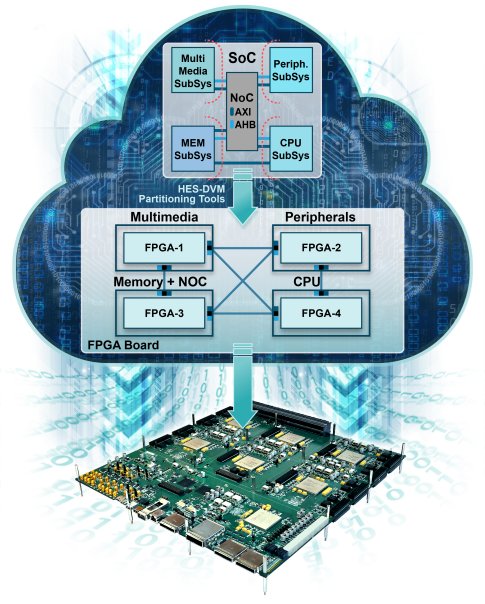
Henderson, NV, USA – June 2, 2021 – Aldec, Inc., a pioneer in mixed HDL language simulation and hardware-assisted verification for FPGA and ASIC designs, has launched HES-DVM Proto Cloud Edition (CE). Available through Amazon Web Service (AWS), HES-DVM Proto CE can be used for FPGA-based prototyping of SoC / ASIC designs and has a focus on automated design partitioning to greatly reduce bring-up time when up to four FPGAs are needed to accommodate a design.
HES-DVM Proto CE can be used with Aldec’s HES pre-silicon prototyping boards, third party boards or platforms users developed in-house and costs just $2,359.50 per month, so is ideal for use on projects with short prototyping phases. Alternatively, for companies with multiple projects on the go, HES-DVM Proto CE is a great way of evaluating HES-DVM before committing to investing in the traditional licensed version.
“We introduced HES-DVM’s automatic FPGA partitioning feature in 2019,” recalls Zibi Zalewski, General Manager of Aldec’s Hardware Division, “and it proved an immediate success because it allows users to automate the setup of multi-FPGA design prototypes, reduce errors and save lots of time.”
Zalewski goes on to say that current SoCs are designed to meet many ASIC type requirements, such as power efficiency, clock distribution, gating and hierarchical bus architecture to assure the highest performance, avoid deadlocks and minimize power demand peaks. He adds: “Meeting these many ASIC requirements calls for a design architecture and hierarchy that rarely fits easily into an FPGA-based prototyping platform because of the way resources need to be allocated and interconnections made. Changing the design hierarchy for the sake of the prototyping stage is to be avoided, so it is important to have a tool which will automatically create balanced partitions - picking and placing module instances across the original design hierarchy. The tool should also provide a fine grade of controllability and advanced analysis for timing critical paths or evaluating alternative FPGA partitioning schemes and their impact on interconnections.
Of equal importance, explains Zalewski, is the automatic handling of I/O connections with LVDS-based serializers to resolve issues caused by limited numbers of FPGA I/Os.
“All of the above wishes of designers are met by our HES-DVM, which is a well-established and trusted EDA tool. Now, HES-DVM Proto CE makes this extremely powerful capability available - at an affordable price and in an easily scalable manner thanks to the ‘on-demand’ cloud operation model - to engineers desperate to reduce their ASIC and SoC design protype bring-up times.”
HES-DVM Proto CE is delivered as an AWS AMI ready-to-use environment with DVM partitioning software and Aldec’s proven SyntHESer fast synthesis engine. Users need only copy the design RTL source code and can start partitioning immediately, avoiding typical IT or software maintenance issues. The highest level of security is assured by Amazon AWS and the strict process of qualifying the AMI for the AWS Marketplace.
HES-DVM Proto CE can be used for prototypes containing up to four Xilinx FPGAs – present on off-the-shelf prototyping boards like Aldec HES, third party or even in-house-developed FPGA boards that are custom-made for a given project and provide features not available on commercial platforms. If a subsequent revision of the project grows and requires more than four partitions, there is a seamless migration path to the on-premises (standard licensed) version of HES-DVM, which can support any number of FPGAs.
Zalewski concludes: “HES-DVM Proto CE is aimed at mid-sized projects with budgets to match. In essence, we’ve made a very affordable version of an extremely powerful and time-saving EDA tool available to users who may not need to be design partitioning year-round.”
HES-DVM Proto CE is now available for purchase.

Aldec launches HES-DVM Proto Cloud Edition (CE). Available through Amazon Web Service (AWS) the cloud-based tool can be used for FPGA-based prototyping of SoC / ASIC designs, and has a focus on automated design partitioning to greatly reduce bring-up time.
About HES™ Prototyping
Aldec offers a portfolio of HES™ prototyping boards based on the largest Xilinx FPGAs of the Virtex UltraScale+, UltraScale and Virtex-7 families. The boards are architected to allow for easy expansion using BPX backplane and standardized FMC and BPX daughter card connectors.
About HES-DVM-CE™
HES-DVM Proto CE is the Cloud Edition of HES-DVM software product used for design compilation and partitioning into multi-FPGA prototyping platforms. It is available from Amazon AWS Marketplace as an Amazon Machine Image (AMI) built upon the Amazon Linux image as a base with preinstalled Aldec HES-DVM software. The HES-DVM Proto CE combines Electronic Design Automation software for design partitioning and compute platform scalability of Amazon Elastic Compute Cloud (Amazon EC2).
About Aldec
Aldec Inc., headquartered in Henderson, Nevada, is an industry leader in Electronic Design Verification and offers a patented technology suite including: RTL Design, RTL Simulators, Hardware-Assisted Verification, SoC and ASIC Prototyping, Design Rule Checking, CDC Verification, IP Cores, Requirements Lifecycle Management, DO-254 Functional Verification and Military/Aerospace solutions. www.aldec.com
Related Semiconductor IP
- ASIL B Compliant MIPI CSI-2 CSE2 Security Module
- SHA-256 Secure Hash Algorithm IP Core
- EdDSA Curve25519 signature generation engine
- DeWarp IP
- 6-bit, 12 GSPS Flash ADC - GlobalFoundries 22nm
Related News
- Aldec采用HES-DVM Proto模式缩短了FPGA的ASIC设计原型开发时间
- Aldec在2017年嵌入式视觉峰会上推出了最新的基于赛灵思Zynq的TySOM嵌入式原型设计板
- Xilinx 发布数据中心生态系统投资计划 致力于进一步壮大云计算及 NFV 加速解决方案
- Linaro发布基于云端的ARM的开发环境