High-speed IP for TSMC
Welcome to the ultimate
High-speed IP
for
TSMC
hub! Explore our vast directory of
High-speed IP
for
TSMC
All offers in
High-speed IP
for
TSMC
Filter
Compare
83
High-speed IP
for
TSMC
from
14
vendors
(1
-
10)
-
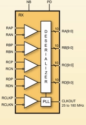
LVDS Deserializer IP
- The MXL-DS-LVDS is a high performance 4-channel LVDS Deserializer implemented using digital CMOS technology.
- Both the serial and parallel data are organized into four channels. The parallel data can be 7 or 10 bits wide per channel. The input clock is 25MHz to 165MHz. The De-serializer is highly integrated and requires no external components.
-
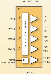
LVDS Serializer IP
- The MXL-SR-LVDS is a high performance 4-channel LVDS Serializer implemented using digital CMOS technology. Both the serial and parallel data are organized into four channels.
- The parallel data width is programmable, and the input clock is 25MHz to 165MHz. The Serializer is highly integrated and requires no external components.
-
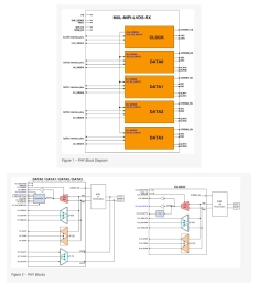
MIPI D-PHY/LVDS Combo Receiver IP
- The MXL-LVDS-MIPI-RX is a high-frequency, low-power, low-cost, source-synchronous, Physical Layer that supports the MIPI® Alliance Standard for D-PHY and compatible with the TIA/EIA-644 LVDS standard.
- The IP is configured as a MIPI slave and consists of 5 lanes: 1 Clock lane and 4 data lanes, which make it suitable for display serial interface applications (DSI).
-
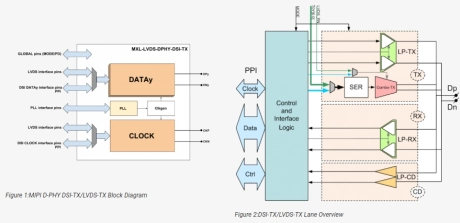
MIPI D-PHY/LVDS Combo Transmitter IP
- The MXL-LVDS-DPHY-DSI-TX is a combo PHY that consists of a high-frequency low-power, low-cost, source-synchronous, Physical Layer supporting the MIPI® Alliance Standard for D-PHY and a high performance 4-channel LVDS Serializer implemented using digital CMOS technology.
- In LVDS mode, both the serial and parallel data are organized into 4 channels. The parallel data is 7 bits wide per channel. The input clock is 25MHz to 150MHz. The serializer is highly integrated and requires no external components. The circuit is designed in a modular fashion and desensitized to process variations. This facilitates process migration, and results in a robust design.
-
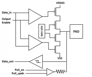
Ultra-low leakage I/O Library in TSMC 22nm
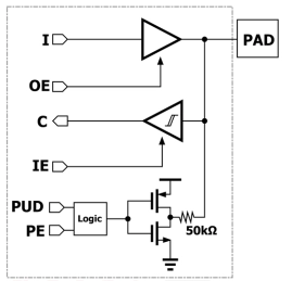
- A TSMC 22nm Wirebond I/O Library with ultra-low leakage 1.8V GPIO, 1.8V I2C ODIO, 1.8V analog cell and associated ESD.
- This is an ultra-low leakage library. The GPIO has a typical leakage of only 150pA from VDDIO and 1nA from VDD.
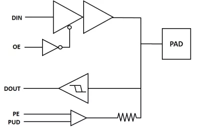
- The library has a GPIO and an ODIO. The GPIO cell set can be configured as input or output and has an internal 50K ohm pull-up or pull-down resistor.
-
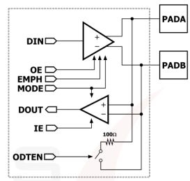
2Gbps LVDS/SVLS Combo Transceiver in TSMC 16nm
- AD_SLVS_LVDS is a highly configurable 2Gbps transceiver for LVDS or SLVS interfaces. With features like dynamic interface selection, on-die termination and pre-emphasis, this I/O is flexible enough for any system.
- To compliment this I/O, the vendor also offers a accompanying silicon-proven ESD and GPIO pad library in TSMC 12/16nm.
- This I/O provides 2kV HBM protection but can be extended up to 8kV upon request.
-
LVDS Transceiver in TSMC 28nm
- This 1.8V LVDS transceiver, designed for TSMCs 28nm process, delivers high-speed, low-power differential signaling with superior signal integrity.
- Engineered with 1.8V thick oxide devices and a 0.8V standard core interface, it operates ef- ficiently across a wide temperature range (-40°C to 125°C).
-
1.8V/3.3V Switchable GPIO with I2C, HDMI, LVDS, ESD & Analog in TSMC 28nm
- A TSMC 28nm HPM/HPC/HPC+ Wirebond I/O Library with a switchable 1.8V/3.3V GPIO, 5V I2C ODIO, 1.8V & 3.3V Analog Cells, ESD and more.
- A key attribute of this silicon-proven library is to detect and adjust to a VDDIO supply of 1.8V or 3.3V during system operation.
- The GPIO can be configured as input, output, open-source, or open-drain with an optional 60kohm pull-up or pull-down resistor.
-
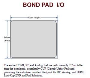
HDMI, LVDS, RF and Analog Pads in TSMC 45/40nm
- A 1.0V to 5V Analog I/O library that includes an HDMI, LVDS, and Analog/RF Low Capacitance pad set in TSMC 45/40nm HPM process.
- This library is collection of analog only IO and Power/Ground pads that include ESD. The target applications are high performance analog interfaces including HDMI, RF, LVDS, basic analog and other applications.
- The pads include a host of specialty features including fail safe, low capacitance, high ESD protection, and IEC robustness.
-
2.5V GPIO with 2Gbps LVDS RX TX and Analog Cell in GlobalFoundries 65nm LPe
- A GlobalFoundries 65nm LPE Wirebond I/O library with 2.5V GPIO, 2Gbps LVDS TX RX and 2.5V Analog/RF cell with associated ESD.
- A key attribute of this silicon-proven library include dual selectable drive strengths and independent input & output enable / disable.
- The GPIO cell can be configured as input, output or open-drain with a Schmitt trigger input and selectable internal 60K ohm pull-up or pull-down resistor.