Interface IP Cores for Silterra
-
I2C Controller IP – Master, Parameterized FIFO, AXI Bus
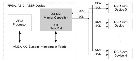
- The DB-I2C-M-AXI Controller IP Core interfaces an ARM, MIPS, PowerPC, ARC or other high performance microprocessor via the AMBA 2.0 AXI System Interconnect Fabric to an I2C Bus. The I2C is a two-wire bidirectional interface standard (SCL is Clock, SDA is Data) for transfer of bytes of information between two or more compliant I2C devices, typically with a microprocessor behind the master controller and one or more slave devices.
- The DB-I2C-M-AXI is a Master I2C Controller that controls the Transmit or Receive of data to or from slave I2C devices. Figure 1 depicts the system view of the DB-I2C-M AXI Controller IP Core embedded within an integrated circuit device.
-
I2C Controller IP- Master / Slave, Parameterized FIFO, AHB Bus
-
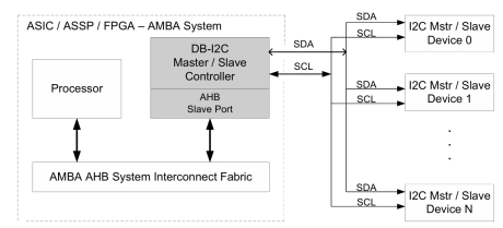
The DB-I2C-MS-AHB Controller IP Core interfaces a microprocessor via the AMBA AHB Bus to an I2C Bus in Standard-Mode (100 Kbit/s) / Fast-Mode (400 Kbit/s) / Fast-Mode Plus (1 Mbit/s) / Hs-Mode (3.4+ Mb/s) / Ultra Fast-Mode (5 mbit/s).
The I2C is a two-wire bidirectional interface standard (SCL is Clock, SDA is Data) for transfer of bytes of information between two or more compliant I2C devices, typically with a microprocessor behind the master controller and one or more slave devices.
The DB-I2C-MS-AHB is a Master / Slave I2C Controller that in Master Mode controls the Transmit or Receive of data to or from slave I2C devices while in Slave Mode allows an external I2C Master device to control the Transmit or Receive of data.
-
-
I2C Controller IP- Master / Slave, Parameterized FIFO, APB Bus
-
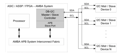
The Digital Blocks DB-I2C-MS-APB Controller IP Core interfaces a microprocessor via the AMBA APB Bus to an I2C Bus in Standard-Mode (100 Kbit/s) / Fast-Mode (400 Kbit/s) / Fast-Mode Plus (1 Mbit/s) / Hs-Mode (3.4+ Mb/s) / Ultra Fast-Mode (5 mbit/s).
The I2C is a two-wire bidirectional interface standard (SCL is Clock, SDA is Data) for transfer of bytes of information between two or more compliant I2C devices, typically with a microprocessor behind the master controller and one or more slave devices.
The DB-I2C-MS-APB is a Master/Slave I2C Controller that in Master Mode controls the Transmit or Receive of data to or from slave I2C devices while in Slave Mode allows an external I2C Master device to control the Transmit or Receive of data.
-
-
I2C Controller IP- Master / Slave, Parameterized FIFO, AXI Bus
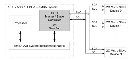
- The DB-I2C-MS-AXI Controller IP Core interfaces a microprocessor via the AMBA AXI Bus to an I2C Bus in Standard-Mode (100 Kbit/s) / Fast-Mode (400 Kbit/s) / Fast-Mode Plus (1 Mbit/s) / Hs-Mode (3.4+ Mb/s) / Ultra Fast-Mode (5 mbit/s).
- The I2C is a two-wire bidirectional interface standard (SCL is Clock, SDA is Data) for transfer of bytes of information between two or more compliant I2C devices, typically with a microprocessor behind the master controller and one or more slave devices.
- The DB-I2C-MS-AXI is a Master / Slave I2C Controller that in Master Mode controls the Transmit or Receive of data to or from slave I2C devices while in Slave Mode allows an external I2C Master device to control the Transmit or Receive of data.
-
PHY layer solution for PCIe1.1/PCIe2.0 with a serial interface and PIPE3 compliant digital interface
- Support for 2.5Gbps/5.0Gbps data rate for PCIe1.1 and PCIe2.0
- Support Loop-back BERT and Loop-back
- Support Self-calibration for On-die-termination
-
Dual FPD-link, 30-Bit Color LVDS Transmitter, 40-170Mhz (Full-HD @120Hz) - with 2 independant links capability LVDS SerDes 70:10 channel compression
- 1P6M/1P7M/1P8M layout structure based on 0.13um Logic 1P8M Salicide 1.2V/3.3V process.
- 1.2V/3.3V ±10% supply voltage, -40/+125°C
- Complies with OpenLDI specification for digital display interfaces and LVDS IEEE Standard 1596.3-1996+ ANSI/TIA/EIA-644-A Specifications.
- Up to 11.9Gbps bandwidth (40 to 170Mhz pixel clock) per pixel channel (Full HD @ 120Hz)
-
FPD-link, 30-Bit Color LVDS Receiver, 20-112Mhz (SVGA/WXGA/SXGA) LVDS SerDes 5:35 channel decompression
- Layout structure based on 1P6M, 1P7M, or 1P8M 0.13um Logic Salicide 1.2V/3.3V process.
- 1.2V/3.3V ±10% supply voltage, -40/+125°C
- Complies with OpenLDI specification for digital display interfaces and LVDS IEEE Standard 1596.3-1996+ ANSI/TIA/EIA-644-A Specifications.
- Up to 3.15Gbps bandwidth (20 to 90Mhz pixel clock)
-
FPD-link, 30-Bit Color LVDS Receiver, 40-170Mhz (Full-HDTV @60Hz) LVDS SerDes 5:35 channel decompression with deskew capability
- Layout structure based on 1P6M, 1P7M, or 1P8M 0.13um Logic Salicide 1.2V/3.3V process.
- 1.2V/3.3V ±10% supply voltage, -40/+125°C
- Complies with OpenLDI specification for digital display interfaces and LVDS IEEE Standard 1596.3-1996+ ANSI/TIA/EIA-644-A Specifications.
- Up to 5.6Gbps bandwidth (40 to 170Mhz pixel clock) ( supports Full HDTV 1080p )
-
LVDS serdes 4:28 channel decompression RX 8-150Mhz
- FPD-LINK Receiver (also available in 30bits color 150Mhz dual channel)
- - 4:28 Data channel decompression up to 1050mb /lane
- - Wide Frequency Range: 8 - 150MHz suited for VGA,SVGA,XGA and SXGA
- - Narrow bus (10 lines) reduces cable size
-
LVDS serdes 28:4 channel compression TX 20-170Mhz
- FPD-LINK Transmitter ( lowest pad count compare to other IP provider )
- 28:4 Data channel compression up to 1190Mbs/channel
- Wide Frequency Range: 20 - 170MHz (single channel) suited for VGA,SVGA,XGA and SXGA
- Narrow bus (10 lines) reduces cable size