The Arasan USB 2.0 PHY IP core is a transceiver compliant with the USB 2.0 Transceiver Macrocell Interface Plus (UTMI+) level 3 specification, for use with host, embedded host, On-the-Go (OTG) and function controllers. Its high speed, mixed-signal circuitry supports 480 Mb/s USB 2.0 High Speed (HS) traffic, while remaining backward compatible with USB 1.1 legacy protocol for 12Mb/s Full Speed (FS) traffic and 1.5Mb/s Low Speed (LS) traffic.
The USB 2.0 PHY performs low-level protocol and signaling functions. While transmitting, the PHY serializes data, generates Synchronize (SYNC) and End-of-Packet (EOP) packet fields, and performs bit stuffing and Non-Return-to-Zero Inverted (NRZI) encoding. While receiving data, the PHY recovers incoming data and clock, de-serializes data, strips SYNC and EOP fields, and performs bit unstuffing and NRZI decoding.
The USB 2.0 PHY is a full-featured on-chip physical transceiver. It has Electro Static Discharge (ESD) protection and fully supports all OTG and host functionality. An optional charge pump generates a 5V supply to power external USB peripherals while in host mode. On-board clock generation and PLL blocks provide for accurate, high-speed data transmission from and to the transceiver. When this USB PHY core is used, a minimal number of external components is required.
USB 2.0 PHY
Overview
Key Features
- Complies with USB specifications, rev. 2.0 and 1.1
- Complies with UTMI+ specification, level 3, rev. 1.0
- Supports 480Mb/s (HS), 12Mb/s (FS) and 1.5MB/s (LS) serial data transmission rates
- Supports 8-bit unidirectional Parallel Interface Engine (PIE) bus for HS, FS and LS modes, and Serial Interface Engine (SIE) for FS and LS modes
- Supports USB 2.0-defined test modes
- Supports OTG USB 2.0
- Supports single-ended data interface
- Digital I/O for Tx and Rx USB OTG cable status
- Rail-to-rail common mode differential receiver
- NRZI encoding and decoding
- SYNC and EOP generation and detection
- Bit stuffing and un-stuffing with error detection
- Optional Charge Pump
- Short-circuit protection for Charge Pump
- Supports full junction temperature range of -40°C to 125°C
- Dual 3.3V/1.2V supply
- Integrated HS and FS/LS terminations
- Area <1mm2 at 130nm
- On-chip decoupling capacitors to minimize digital switching noise
Benefits
- Silicon proven
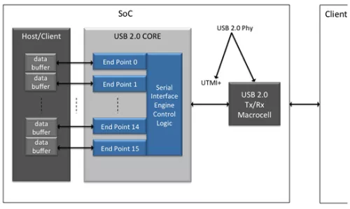
Block Diagram
Deliverables
- GDSII layout and layer map
- Place-and-route views (.lib, .lef)
- LVS and DRC verification reports
- Verilog Sim Model (NC-Verilog)
- Gate-level netlist and SDF timing
- Test guidelines, layout guidelines and application notes
Technical Specifications
Maturity
Silicon proven
Availability
Now