PCIe Gen 2 Verification IP

Overview

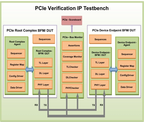
The PCIe Gen2 Verification IP provides an effective & efficient way to verify the components interfacing with PCIe Gen2 interface of an IP or SoC.

The PCIe Gen2 VIP is fully compliant with standard PCIe Gen2 specifications. This VIP is a light weight with an easy plug-and-play interface so that there is no hit on the design cycle time.

Key Features

  • Compliant with PCI Express Specifications 2.0 (5GT/s) and 1.1 (2.5GT/s).
  • Verification IP configurable as PCI express Root Complex and Device Endpoint.
  • Configurable LinkWidth: x1, x2, x4, x8, x12, x16, x32.
  • Configurable pipe width : 8,16,32,64
  • On the fly change in link speed, link width and pipe width through single testcase..
  • Supports split a port to more than one link - multi link.
  • Supports Low Power management LTSSM states - L0s, L1, L2 , PCI-PM, ASPM.
  • User Configurable fields -SKP interval count, FTS transmission count.
  • Support for on the fly change in linkspeed and linkwidth through single test.
  • Configurable number of virtual channels(VCs) : Single VC / Multiple VCs( 1-7).
  • Configurable number of functions.
  • Supports 128B, 256B, 512B, 1kB, 2KB or 4kB Maximum Payload Size (MPS).
  • Supports for multifunction and SR-IOV with configurable number of Virtual functions
  • Supports ATS with lastest specification version 1.1
  • Interrupt support: INTx or MSI MSI-X and ECAM support.
  • Advanced Error Reporting (AER) with optional Malformed TLP checks, ECRC and TLP Poisoning support.
  • Compliance testing in TL, DLL & PL including power management test-suites.
  • On the fly protocol checking using protocol check functions, static and dynamic assertion.
  • Built in Coverage analysis.
  • Provides a comprehensive user API (callbacks).
  • Graphical analyser for all three Layers to show PCIe transactions for easy debugging.
  • Supports FLR ( Function Level Reset).

Block Diagram

PCIe Gen 2 Verification IP  
 Block Diagram

Technical Specifications

×
Semiconductor IP