Efficient logic optimization utilizing complementary behavior of CMOS gates
By Gaurav Goyal, Abhishek Mahajan, Sidhartha Taneja (Freescale Semiconductor)
Any typical digital design style with CMOS uses complementary pairs of p-type and n-type MOSFETs for logic functions implementation. Naturally, CMOS always ought to provide INVERTED outputs like Inverter, NAND, NOR etc. Sometimes a non-inverting function is required, in which case it's just as easy to implement it with a final inverter or with a non-inverting function like AND, OR as also shown in the below Fig. 1
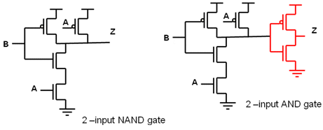
Fig. 1 NAND inverting gate and AND non-inverting gate
Standard CMOS gates used in IC design are inverting for a variety of reasons, including lower area and delay compared to the non inverting versions. So, It would be inefficient to use an inverter when the inversion can be optimized away in the logic by using an inverting logic function such as NAND, NOR etc. (Inverting logic being preferred).
It has been seen that even after the logic restructuring with tools, there are multiple scenarios where an “inverting function” has been implemented with “non-inverting function + inverter”; which is inefficient & creates an opportunity to optimize in terms of area/timing/power by replacing the “non-inverting function + inverter” combination with “inverting function + inverter” combination thus saving an inverter.
There are millions of such scenarios in any design and below is one of the cases where such inefficiency can be seen:

Fig. 2 Scenario depicting inverter being used after the non-inverting logic
Proposed Approach: Replace “non-inverting function + inverter” combination with “inverting function + inverter” combination thus saving an inverter as below.

Fig. 3 Conventional v/s Proposed Approach saves ‘1’ inverter
While doing so, there is a need to keep a tab on certain things for its successful implementation like:
- Check if the cell corresponding to inverting functionality of Inverter’s-driver (non-inverting functionality) exists in standard cell library, then only such swapping is possible.
- If Timing slack and DRV has sufficient slack available and physical net length is < 30um (depends on technology to technology), do the required swapping so as to ensure that inverter was not used for DRV fixing.
Conclusion:
There is a saving of ‘1’ inverter for every such scenario present which would save area/power & relaxes the timing further & comes with no-side effect as well.
Related Semiconductor IP
- ReRAM NVM in DB HiTek 130nm BCD
- UFS 5.0 Host Controller IP
- PDM Receiver/PDM-to-PCM Converter
- Voltage and Temperature Sensor with integrated ADC - GlobalFoundries® 22FDX®
- 8MHz / 40MHz Pierce Oscillator - X-FAB XT018-0.18µm
Related Articles
- Asynchronous Logic: large CMOS devices without a clock tree
- An Efficient Software-Hardware Partitioning for Transport Demultiplexer
- Efficient methodology for design and verification of Memory ECC error management logic in safety critical SoCs
- Efficient SIMD and Algorithmic Optimization Techniques for H264 Decoder on Cortex A9
Latest Articles
- An FPGA-Based SoC Architecture with a RISC-V Controller for Energy-Efficient Temporal-Coding Spiking Neural Networks
- Enabling RISC-V Vector Code Generation in MLIR through Custom xDSL Lowerings
- A Scalable Open-Source QEC System with Sub-Microsecond Decoding-Feedback Latency
- SNAP-V: A RISC-V SoC with Configurable Neuromorphic Acceleration for Small-Scale Spiking Neural Networks
- An FPGA Implementation of Displacement Vector Search for Intra Pattern Copy in JPEG XS