VLSI implementation of OFDM modem
by Aseem Pandey, Shyam Ratan Agrawalla & Shrikant Manivannan
from Wipro Technologies
Abstract
OFDM is a multi-carrier system where data bits are encoded to multiple sub-carriers, while being sent simultaneously. This results in the optimal usage of bandwidth. A set of orthogonal sub-carriers together forms an OFDM symbol. To avoid ISI due to multi-path, successive OFDM symbols are separated by guard band. This makes the OFDM system resistant to multi-path effects.
Although OFDM in theory has been in existence for a long time, recent developments in DSP and VLSI technologies have made it a feasible option. Many wired and wireless standards like DVBT, DAB, xDSL and 802.11a have adopted OFDM.
This paper first lists various approaches to implement an OFDM system. It then describes the VLSI implementation of OFDM in details. Specifically the 802.11a OFDM system has been considered in this paper. However, the same considerations would be helpful in implementing any OFDM system in VLSI.
Introduction
OFDM is a multi-carrier system where data bits are encoded to multiple sub-carriers. Unlike single carrier systems, all the frequencies are sent simultaneously in time. OFDM offers several advantages over single carrier system like better multi-path effect immunity, simpler channel equalization and relaxed timing acquisition constraints. But it is more susceptible to local frequency offset and radio front-end non-linearities. The frequencies used in OFDM system are orthogonal. Neighboring frequencies with overlapping spectrum can therefore be used. This property is shown in the figure where f1, f2 and f3 orthogonal. This results inefficient usage of BW. The OFDM is therefore able to provide higher data rate for the same BW
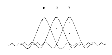
OFDM is fast gaining popularity in broadband standards and highspeed wireless LAN.
OFDM transceiver
Each sub-carrier in an OFDM system is modulated in amplitude and phase by the data bits. Depending on the kind of modulation technique that is being used, one or more bits are used to modulate each sub-carrier. Modulation techniques typically used are BPSK, QPSK, 16QAM, 64QAM etc. The process of combining different sub-carriers to form a composite time-domain signal is achieved using Fast Fourier transform. Different coding schemes like block coding, convolutional coding or both are used to achieve better performance in low SNR conditions. Interleaving is done which involves assigning adjacent data bits to non-adjacent bits to avoid burst errors under highly selective fading. Block diagram of an OFDM transceiver is shown below.
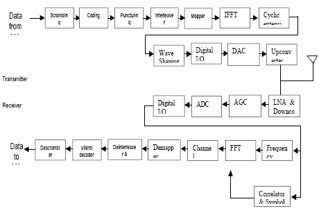
Figure 1: Block diagram of the 802.11a OFDM transceiver
Different implementation techniques
Figure 1 shows an OFDM transciever. Following choices are available for imple menting an OFDM system.
- DSP based implementation
- DSP based implementation with hardware accelerators
- VLSI implementation
The pros and cons of each approach are explained in the following sections.
DSP based implementation
High performance Digital Signal Processors are widely available in the market today. The computer-intensive and time critical functions that were traditionally implemented in hardware are now being implemented in the software running on these processors.
Implementing the entire OFDM transceiver in software on DSPs is thus an option to be considered for some applications.
It has the following advantages:
- Reduced development time and quick prototyping. Quick time to market.
- Flexibility. It can quickly adapt to changing or different standards as it needs only a software change.
- Ideal for multi-mode Basebands where multiple standards are supported by the same device
DSP based implementation has the following disadvantages:
- Not very optimum in terms of area and power consumption
- High MIPS requirement.
The approximate MIPS requirement for different blocks in OFDM is given below.
| Module | MIPS |
| Viterbi decoder | 4000 |
| FFT | 500 |
| NCO | 120 |
| Interleaver | 150 |
| Channel compensation | 100 |
| Scrambler & others | 50 |
The total MIPS requirement is 4500+. Such high CPU power is not available even with the fastest DSPs in the market today. One way out is parallel processing with multiple DSPs as shown in figure
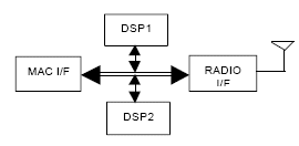
Figure 2: DSP solution
DSP with hardware accelerators
To overcome the MIPS limitation and yet to retain the flexibility of software implementation, some blocks can be implemented in H/W. Figure 3 shows an implementation which can reduce the MIPS requirement by around 4000 MIPS.
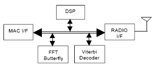
Figure 3: DSP + H/W accelerators
VLSI implementation

Figure 4: VLSI Implementation
In the approach shown in Figure 4 the entire functionality is implemented in hardware.
Following are the advantages of this approach:
- Lower gate count compared to DSP+RAM+ROM, hence lower cost
- Low power consumption
Due to the advantages mentioned above a VLSI based approach was considered for implementation of an 802.11a Baseband. Following sections describe the VLSI based implementation in details.
Design Methodology
The design approach for the OFDM modem is slightly different than a typical ASIC flow. Early in the development cycle, different communication and signal processing algorithms are evaluated for their performance under different conditions like noise, multipath channel and radio non-linearity. Since most of these algorithms are coded in “C” or tools like Matlab, it is important to have a verification mechanism which ensures that the hardware implementation (RTL) is same as the “C” implementation of the algorithm. The flow is shown in the Figure 5.
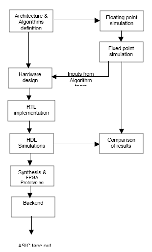
Figure 5: Design flow for Baseband development
Architecture definition
Following points need to be considered in the architecture definition phase.
Specifications of the OFDM transceiver
- Data rates to be supported
- Range and multipath tolerance
- Indoor/Outdoor applications
- Multi-mode: 802.11a only or 802.11a+HiperLAN/2
Design trade-offs
- Area – Smaller the die size lesser the chip cost
- Power – Low power crucial for battery operated mobile devices
- Ease of implementation – Easy to debug and maintain
- Customizability – Should be customizable to future standards with variations in OFDM parameters
Algorithm survey & simulation
The simulation at algorithmic level is to determine performance of algorithms for various non-linearities and imperfections. The algorithms are tweaked and fine tuned to get the required performance. The following algorithms/parameters are verified.
- Channel estimation and compensation for different channel models (Rayleigh, Rician, JTC, Two ray) for different delay spreads
- Correlator performance for different delay spreads and different SNR (AWGN model)
- Frequency estimation algorithm for different SNR and frequency offsets
- Compensation for Phase noise and error in Frequency offset estimation
- System tolerance for I/Q phase and amplitude imbalance
- FFT simulation to determine the optimum fixed-point widths
- Wave shaping filter to get the desired spectrum mask
- Viterbi BER performance for different SNR and traceback length
- Determine clipping levels for efficient PA use
- Effect of ADC/DAC width on the EVM and optimum ADC/DAC width
- Receive AGC
Fixed point simulation
One of the decisions needs to be taken early in the design cycle is the format or representation of data. Floating point implementation results in higher hardware costs and additional circuits related with normalizing of numbers. Floating point representa tion is useful when dealing with data of different ranges. However, this is not true as the Baseband circuits have a fair idea of the range of values that they will work on. So a fixed-point representation will be more efficient. Further in fixed point a choice can be made between signed and 2's complement representation.
The width of representation need not be constant throughout the Baseband and it depends on the accuracy needed at different points in transmit or receive path. A small change in the number of bits in the representation could result in a significant change in the size of arithmetic circuits especially multipliers.
| Module | Width | Gate count |
| Complex | 12 | 6K |
| Multiplier | 16 | 10K |
| FFT (Radix-4 with 3 complex multipliers) | 12 | 24 K (excluding RAM) |
| 16 | 36 K (excluding RAM) |
Shown below is the loss of SNR due to the decrease in the width of representation.
| Module | Width | SNR dB (Signal to Quantization noise ratio) |
| ADC | 8 | 48 |
| 12 | 72 |
Simulations for different bit-widths tell us which is the optimum bit-width that main tains the required level of accuracy. Significant area and power savings could be made if accurate estimation of fixed-point widths is made. Simulations are performed to determine the required precision.
Simulation setup
The algorithms could be simulated in a variety of tools/languages like SPW, MATLAB, “C” or a mix of these.
SPW has an exhaustive floating point and fixed-point library. SPW also provides feature to plug-in RTL modules and do a co-simulation of SPW system and Verilog. This helps in verifying the RTL implementation of algorithms against the SPW/C implementation.
Hardware design
Interface definition
Baseband interfaces with two external modules: MAC and Radio.
Interface to MAC
- Baseband should support the following for MAC
- Should support transfer of data at different rates
- Transmit and receive control
- RSSI/CCA indication
- Register programming for power and frequency control
- Following options are available for MAC interface:
- Serial data interface – Clock provided along with data. Clock speed changes for different data rates
- Varying data width, single speed clock – The number of data lines vary accord ing to the data rate. The clock remains same for all rates.
- Single clock, Parallel data with ready indication – Clock speed and data width is same for all data rates. Ready signal used to indicate valid data
- Interfaces like SPI/Micro-wire/JTAG could be used for register programming
Radio
Two kinds of radio interfaces are described below
I/Q interface
On the transmit side, the complex Baseband signal is sent to the radio unit that first does a Quadrature modulation followed by up-conversion at 5 GHz. On the receive side, following the down-conversion to IF, Quadrature demodulation is done and complex I/Q signal is sent to Baseband. Shown below is the interface.
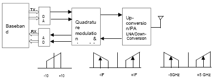
Figure 6: I/Q interface to Baseband
IF interface
The Baseband does the Quadrature modulation and demodulation digitally.
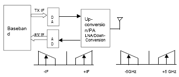
Figure 7: IF interface to Baseband
| I/Q interface | IF interface |
| I/Q Phase/Amplitude imbalance is an issue as the modulation/demodulation is done in analog | No phase imbalance as Quadrature components are produced digitally |
| Two ADC/DAC channels required for I/Q | Single ADC/DAC channel required |
| Sampling frequency is lower (>BW) | Higher sampling frequency needed (>2BW) |
| DC-offset introduced by I/Q ADC has to be compensated | DC-offset introduced at the receiver ADC is not a problem as there is a mixing stage inside |
Clocking strategy
The 802.11a supports different data rates from 6 Mbps to 54 Mbps. The clock scheme chosen for the Baseband should be able to support all rates and must also result in low power consumption. We know from our Basic ASIC design guidelines that most circuits should run at the lowest clock.
Two options are shown below:

- Above scheme requires different clock sources or a very high clock rate from which all these clocks could be generated.
- The modules must work for the highest frequency of 54 MHz.

- Shown in the previous figure is a simpler clocking scheme with only one clock speed for all data rates
- Varying duty cycles for different data rates is provided by the data enable signal
- All the circuits in the transmit and receive chain work on parallel data (4 bits)
- Overhead is the Data enable logic in all the modules
Design of crucial blocks
FFT
Requirement: 64 point FFT computation in 4 us as the 802.11a OFDM symbol including the guard interval is 4 us wide.
Figure 8: 64 point Radix-4 FF T data flow diagram
1.1.1.1 Different architectures
- Radix-4 Single-Path delay commutator
- Radix-4 Multi-Path delay commutator
- Radix-4 Single-Path delay feedback
- Pipelined or non-pipelined
1.1.1.2 FFT storage
- Using single RAM – As only one RAM is available, large delays occur because of read and write cycles and therefore faster clock is required to meet FFT time requirement of 4 us
- Using multiple storage, Data load/store happens in parallel, FFT Radix-4 utilization is improved and FFT computation time is less
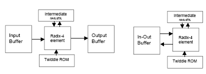 Figure 9: Different storage schemes for FFT
Twiddle factor complex multiplication
Comparison shown for two options
1.1.1.4 Butterfly construction
Since multipliers are the biggest block in Radix-4 butterfly, designer may choose to have 1, 2 or 3 complex multiplier instances based on clock, timing and latency requirements. Shown below are both the kinds
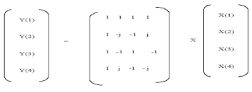
Figure 10: Butterfly operation
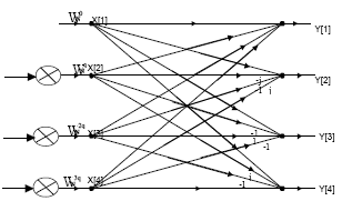
Figure 11: Lower latency with three parallel multipliers
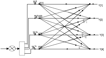
Figure 12: Single complex multiplier, higher latency (or higher clock required for same latency)
Viterbi
The ½ , length 7, convolutionally encoded stream is decoded using a Viterbi decoder.

Figure 13: Viterbi Construction
1.1.1.5 BMU
Branch metrics computation unit calculates the hamming distances for the incoming pair of codes from four possible codes
1.1.1.6 ACS
Add, compare and select unit is used to update the path metric for all the 64 states and to select the predecessor. For each of the 64 states, it adds current path metric and branch metric for both the predecessor states and selects the lower of the two as the new path metric and the predecessor information is passed on to the SMU unit.
The width of the Path metric register and the ACS adders and subtractor will change based on whether a soft-decision or a hard-decision viterbi is ued. It also depends on the maximum metrics accumulated by metrics registers before a normalization is done.
1.1.1.7 SMU
Survivor metrics unit can be implemented by register-exchange or traceback memory method.
| Register-exchange | Traceback memory |
| Data bits for all possible paths in the trellis are stored in Flip-flops | Decision bits are stored in traceback RAM |
| Low latency = Traceback length | High latency = 4 x Traceback length |
| High gate count =~ 60 K for traceback length of 64 | Low gate count =~25K + 256x64 RAM required |
| High power consumption because of operation of all Flip-flops | Low power consumption |
NCO
NCO (Numerically controlled oscillator) is used for frequency offset correction. NCO generates sine and cosine waves that are mixed with the incoming Baseband signal to correct the frequency error. Various design parameters to be decided in NCO are given below
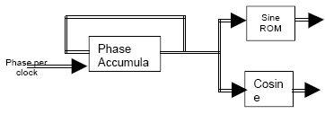
Figure 14: NCO
Width of phase-accumulator. Will decide on the accuracy or “ppm” of generated waveform
Width of Sine and cosine outputs. Decides Quantization error. But this also decides the size of ROM used to keep the sine and cosine tables
By using the fact the cos (q) = sin (90 - q), a single LUT can be used to generate both sine and cosine values
The need for Sine/Cosine ROM can be eliminated by using a CORDIC rotator (if the pipeline delay that the CORDIC introduces can be tolerated).
Arctan
The tan-1 circuit is used during the estimation of the frequency error caused by local frequency PPM errors. This could be implemented as a simple LUT, which contains the Arctan values for different angles or it can be implemented by using a CORDIC circuit in vectoring mode. CORDIC is an abbreviation for Coordinate rotation digital computer. It involves performing the following equations iteratively.
Let us say the complex vector is x0 + jy0 and our objective is to find z = tan-1(y0/x0), it can be achieved by doing the following.
xi+1 = xi – yi*di*2-i
yi+1 = yi + xi*di*2-i
zi+1 = zi – di*tan-1(2-i).
Where
di = +1 if yi < 0, -1 otherwisi eis the iteration number and decides the accuracy of the result. As can be seen, the CORDIC circuit is simple to construct and involves only shifts, additions and subtractions.
| Using LUT | CORDIC |
| Huge RAM needed for high accuracy | Low gate count |
| Low latency | High latency because of iterative method |
CORDIC circuit is preferred as it results in a low gate count implementation.
Optimize usage of hardware resources by reusing different blocks
Hardware resources can be reused considering the fact that 802.11a system is a halfduplex system. The following blocks are re-used
FFT/IFFT
- Interleaver/De-interleaver
- Scrambler/Descrambler
- Intermediate data buffers
Since Adders and Multipliers are costly resources, special attention should be given to reuse them. An example shown below where an Adder/Multiplier pool is created and different blocks are connected to this.
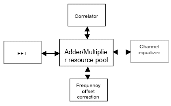
Figure 15: Sharing of H/W resources
Optimize the widely used circuits
Identify the blocks that are used at several places (several instances of the same unit) and optimize them. Optimization can be done for power and area. Some of the circuits that can be optimized are:
Multipliers
They are the most widely used circuits. Synthesis tools usually provide highly optimized circuits for multipliers and adders. In case optimized multipliers are not available, multipliers could be designed using different techniques like booth- (Non) recoded Wallace.
ACS unit
There are 64 instantiations of ACS unit in the Viterbi decoder. Optimization of ACS unit results in significant savings. Custom cell design (using foundry information) for adders and comparators could be considered.
Debug support
- To enable debugging the hardware a serial port or a parallel port interface could be provided
- The port could be used to control the core, issue transmit and receive com mands, analyzing the receive data for errors, monitoring BER etc
- Test mode support can be provided in the core to facilitate selective testing of the modules inside
RTL Simulations
RTL simulations are conducted to achieve the following objectives:
- Functional verification for all transmit and receive Baseband functions for different data rates is done
- Necessary models are written to introduce noise and channel effects. Verilog PLI interface can be used to plug-in “C” models if they are available
- It is verified that different algorithmic blocks are implemented correctly in RTL, the same set of vectors used in algorithm simulations are applied to the RTL system and the outputs are compared. If simulations for algorithms are done in a tool like SPW, then this can be easily be done by importing the RTL blocks in SPW system
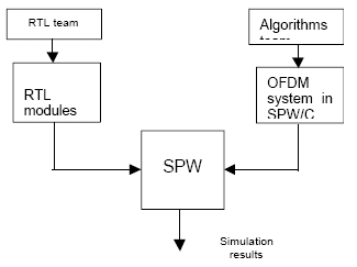
Figure 16: Simulation setup in SPW environment
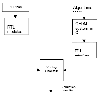
Figure 17: Simulation setup in Verilog environment
After algorithm verification, the verilog RTL code is typically tested on a prototype board using FPGAs before fabricating the ASIC. The details of these activities are outside the scope of this paper.
References
1. ISO/IEC 8802-11 ANSI/IEEE Std 802.11-1999, Part 11: Wireless LAN Medium Access Control (MAC) and Physical Layer (PHY) specifications, IEEE, 20th August 1999
2. IEEE Std 802.11a-1999(Supplement to IEEE Std 802.11-1999), Part 11: Wireless LAN Medium Access Control (MAC) and Physical Layer (PHY) specifications, IEEE, September 1999
3. Digital signal Processing, J.G.Proakis, D.G Manolakis, Third Edition
4. Digital communications, Simon Haykin, John Wiley and sons
5. Very Fast Fourier Transform Algorithms Hardware for Implementation, Alvin M. Despain, IEEE transactions on computers, Vol. c-28 No 5, May 1979
6. Robust Frequency and Timing Synchronization for OFDM, Timothy M. Schmidl and Donald C. Cox, IEEE TRANSACTIONS ON COMMUNICATIONS, VOL. 45, NO. 12, DECEMBER 1997
7. A New Approach for Evaluating Clipping Distortion in Multicarrier Systems, Ahmad R.S. Bahai, Manoneet Singh, Andrea J. Goldsmith, and Burton R. Saltzberg, IEEE JOURNAL ON SELECTED AREAS IN COMMUNICATIONS, VOL. 20, NO. 5, MAY 2002
8. "OFDM for multimedia wireless communications" by Van Nee, Richard and Ramjee Prasad
9. Performance Analysis of Viterbi Decoding for 64-DAPSK and 64-QAM Modulated OFDM Signals, Thomas May, Hermann Rohling, and Volker Engels, IEEE TRANS ACTIONS ON COMMUNICATIONS, VOL. 46, NO. 2, FEBRUARY 1998
10. An Equalization Technique for Orthogonal Frequency-Division Multiplexing Sys tems in Time-Variant Multipath Channels, Won Gi Jeon, Kyung Hi Chang and Yong Soo Cho, IEEE TRANSACTIONS ON COMMUNICATIONS, VOL. 47, NO. 1, JANU ARY 1999
11. Optimum Nyquist Windowing for Improved OFDM Receivers, Stefan H. Muller- Weinfurtner and Johannes B. Huber, Proc. of the IEEE Global Telecommunications Conference GLOBECOM 2000, San Francisco, CA, USA, pp. 711-715, Nov. 2000
Acronyms and definitions
- AGC Automatic gain control
- AWGN Additive white gaussian noise
- BER Bit error rate
- BPSK Binary phase shift keying
- BW Bandwidth
- EVM Error vector magnitude
- FFT Fast Fourier transform
- IF Intermediate frequency
- ISI Inter symbol interference
- PA Power amplifier
- OFDM Orthogonal frequency division multiplexing
- QPSK Quadrature phase shift keying
- QAM Quadrature amplitude modulation
- SPW Signal processing Work-system from Cadence
- SNR Signal to noise ratio
About the Authors
Aseem Pandey is a Senior engineer with the VLSI and Systems design division in Wipro Technologies. He is currently working in a group which develops physical layers of different wireless standards Shyam Ratan Agrawalla is a senior engineer with the VLSI and Systems design division with Wipro Technologies. He is working on the 802.11a OFDM modem development.
Shrikant Manivannan is the technical lead for the 802.11a OFDM modem program at Wipro Technologies. His focus since joining Wipro has been the design of Baseband for different Wireless Standards.
Related Semiconductor IP
- IEEE 802.16 WirelessMAN OFDM Channel Codec
- OFDM - Orthogonal Frequency Division Multiplexing
- Programmable OFDM Channel Estimator
- OFDM synchronization unit
- High Throughput Rate OFDM Baseband PHY Processor
Related Articles
- VLSI Based On Two-Dimensional Reconfigurable Array Of Processor Elements And Theirs Implementation For Numerical Algorithms In Real-Time Systems
- An 800 Mpixels/s, ~260 LUTs Implementation of the QOI Lossless Image Compression Algorithm and its Improvement through Hilbert Scanning
- Evolution of VLSI Technology and its Applications
- Understanding the Importance of Prerequisites in the VLSI Physical Design Stage
Latest Articles
- Extending and Accelerating Inner Product Masking with Fault Detection via Instruction Set Extension
- ioPUF+: A PUF Based on I/O Pull-Up/Down Resistors for Secret Key Generation in IoT Nodes
- In-Situ Encryption of Single-Transistor Nonvolatile Memories without Density Loss
- David vs. Goliath: Can Small Models Win Big with Agentic AI in Hardware Design?
- RoMe: Row Granularity Access Memory System for Large Language Models