Vertically Integrated MIPI Solutions
By Dennis McCarty, Arasan Chip Systems
Overview of the MIPI Standards
The Mobile Industry Processor Interface (MIPI) Alliance is an open-membership organization that includes leading companies in the mobile industry that share the objective of defining and promoting open specifications for interfaces inside mobile terminals. Formed in July 2003 by ARM, Nokia, ST Microelectronics and Texas Instruments, MIPI aims to shave complexity and costs while boosting flexibility for cell phones and other mobile products and the integrated circuits that drive them.
Today there are scores of member companies in the MIPM Alliance and over a dozen working groups developing standards for hardware and software.
Benefits of Using MIPI Standards
The emerging MIPI standards are designed to ensure interoperability among devices and software that are used in products for the exploding hand-held market. The standards facilitate the interconnection of multiple, mixed-signal integrated circuit devices on a single hand-held product. Use of the standards ensures low power, low pin count and interoperability of all the devices in the system and easy integration.
Companies designing mobile products will realize the following benefits from adopting the standards:
- Improve interconnectivity and compatibility
- Reduce fragmentation in mobile product interfaces
- Increase system quality and reliability
- Increase design efficiency
- Maximize design reuse
- Drive innovation
- Reduce time-to-market
- Simplify system integration
MIPI Standards Working Groups
The MIPI standards working groups focus on devices that are used on mobile products such as cameras, displays and radios. Additional working groups focus on related topics including battery management, Physical Layer (PHY) interfaces, test and debug, and the UniPro Link layer. The following sections describe some of the more important standards being developed.
Display Serial Interface (DSI)
The Display Serial Interface Specification defines protocols to transfer data between a host processor and peripheral devices through a D-PHY physical interface. The DSI specification builds on existing specifications by adopting pixel formats and a command set defined in MIPI Alliance specifications for Display Pixel Interface 2 (DPI-2) and Display Command Set (DCS).
The DSI specification defines a high-speed serial interface between a peripheral, such as an active-matrix display module, and a host processor in a mobile device. By standardizing this interface, components may be developed that provide higher performance, lower power, less electromagnetic interference and fewer pins than current devices, while maintaining compatibility across products from multiple vendors.
Camera Standard Interface (CSI)
The Camera Serial Interface 2 specification defines an interface between a peripheral device (camera) and a host processor for mobile device applications.
A host processor in this specification means the hardware and software that performs core functions for telecommunication or application tasks. These include, for example, RF components, basic electronics, and basic software, such as the digital signal processing software.
Unified Protocol (UniPro)
The MIPI Alliance Specification for Unified Protocol (UniPro) defines a layered protocol for interconnecting devices and components within mobile systems such as cellular telephones, handheld computers, digital cameras, and multimedia Devices. The UniPro implements layers L1.5, L2, L3 and L4 protocols and is situated between the PHY and application.
UniPro enables these Devices and components to utilize MIPI PHY layers to exchange data at high data rates, with low pin counts and at low energy per transferred bit. UniPro is applicable to a wide range of component types such as application processors, co-processors, modems, etc. and to different types of data traffic such as control messages, bulk data transfer, packet data streaming.
Implementing the UniPro specification reduces the time-to-market and design cost of mobile devices by simplifying the interconnection of products from different manufacturers. Implementing new features is simplified due to the extensible nature of the UniPro specification.
Physical Layer Devices (PHY)
The physical layer (PHY) is the layer in the communication hierarchy that connects to the physical, analog bus and converts signals to digital data. This PHY specification provides a flexible, low-cost, high-speed serial interface solution for communication interconnection between components inside a mobile device. Traditionally, these interfaces are CMOS parallel busses at low bit rates with slow edges for EMI reasons.
The coming M-PHY solution enables significant extension of the interface bandwidth for more advanced applications. The M-PHY solution can be realized with very low power consumption.
The previous MIPI PHY layer was the D-PHY, but the industry is transitioning to the M-PHY. Both offer either high-speed or low-power signaling. The M-PHY uses fewer pins, but offers faster signaling scaling up to 6 GB/sec. M-PHY also offers more options and flexibility.
Digital Radio frequency (DigRF)
The DigRF specification defines radio communication for mobile devices. The specification covers dual-mode 3GPP 3G / 2.5G (UMTS/EGPRS) mobile terminals. Both modes of operation are supported over a common interface. The interface can also be used for single-mode 3G terminals. The specification defines the interface between a baseband IC (BBIC) and one or more RFICs in a mobile terminal. The interface is intended to be efficient and flexible, accommodating many variations in the overlying system design, while providing interoperability at the interface level between compliant ICs. The key pillars for the design were to:
- Minimize interface pin count
- Minimize overall interface power consumption
- Provide a very reliable physical layer so error correction and detection are not needed.
Serial Low-power Inter-chip Media Bus (SLIMbus)
The SLIMbus specification addresses very low power, low cost peripherals such as keyboards, while being extensible to mid-speed devices. SLIMbus is a scalable and flexible interface designed to evolve with future market needs and demands, while reducing fragmentation and consolidate multiple interfaces.
Common digital audio interfaces used in mobile terminals such as I2S and PCM are generally intended for point-to-point connections between an application processor and a single digital audio device. Typically, these interfaces only support one or two digital audio channels. Adding functions and digital audio channels to mobile terminals beyond those for voice communication and simple stereo music applications is very difficult without increasing the number of bus structures in the mobile terminal. Moreover, adding buses limits design flexibility and increases the costs of pin count, package size, and PCB layout area and power consumption.
SLIMbus provides the industry with a standard, robust, scalable, low-power, high-speed, costeffective, two wire multi-drop interface. SLIMbus supports a wide range of digital audio and control solutions for mobile terminals.
SLIMbus effectively replaces many other digital audio buses such as PCM and I2S, as well as control buses such as I2C, SPI, or UART by providing flexible and dynamic assignment of bus bandwidth between digital audio and non-audio control and data functions. SLIMbus is not backward compatible with any current digital audio bus or digital control.
MIPI Trends & Adoption
The MIPI banner covers such standards as CSI-3, DSI-2, USF, SLIM Bus and others. Handheld system designers employ the standards to add cameras, displays, key boards and so forth to obtain optimal performance and ensure interoperability among vendors of standards devices.
MIPI continues to evolve. The current D-PHY, for example, is yielding to the higher performance M-PHY. CSI-3 is replacing CSI-2 and requires use of a UniPro interface to the controller. Companies that provide MIPI products must be prepared to straddle the standards as they advance and to upgrade their systems once new versions are adopted. The next revision of DSI may also entail use of UniPro as well.
Some elements such as the PHY and UniPro are common to more than one standard. This fact allows an IP product developed or licensed for one standard such as CSI to also be used with another such as UFS. Multiple uses among standards on the same product save development costs, but it puts the onus on the common IP to work with other IP products.
MIPI IP Product Market
Use of IP products speeds product development, not only in design entry, but also in verification and implementation. IP products usually come with a test bench for the standard which can be added to the device-level test bench to verify the entire system. Also included are synthesis scripts to ensure correct implementation.
MIPI standards and the growth of the industry have attracted a number of IP product vendor’s large and small offering products catering to one or more of the standards.
As much as IP has been a boon to developers, the licensing of individual components to build systems entails risks that are magnified as the number suppliers and standards increases for a number of reasons.
As designs have come to incorporate more functionality at greater speed IP users have been vexed by the lack of an integrated, total solution that offers everything from analog to software from a single source. Since most vendors offer piecemeal, point solutions designers have had to deal with multiple vendors in a single project. Typically a designer uses one vendor for the one standard interface and another for a different standard. Integrating these diverse products into a single design is risky and the debugging effort is considerable.
Surveying the MIPI IP market requires customer tenacity. There are a plethora of products offered from vendors large and small. Since implementing most MIPI standards requires multiple IP products the job of selecting vendors is greater than it is with other standards. This job is further magnified by the requirement of many hand-held products for multiple MIPI standards.
The criteria customers should use in selecting a vendor include the range of their MIPI solutions both within and between standards, support, vendor durability and IP interoperability.
Arasan MIPI Product Portfolio
Arasan offers the most comprehensive MIPI solution on the market and, indeed, is the only company to offer all the IP required to implement entire standards. The products range from the physical layer to the software. An example of how Arasan MIMP IP products can be used to build an entire mobile device may be seen in Figure 1.
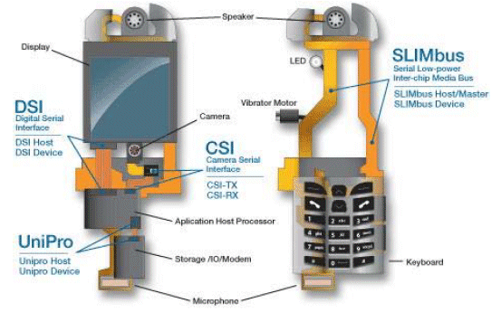
Figure 1: Example of Arasan MIPI Used to Build a Mobile Device
The MIMP solutions include not only digital and analog IP, but also software, VIP, test benches, compliance test vectors and ESL models. Unlike some competitors, the company designs and supports all its products. That ensures a single source for support and guarantees interoperability between all the IP in the system.
The products support the most important standards including UFS, CSI, SLIMbus and DSI along with their supporting physical and link layers as well as system side DMA and bus interfaces. Because it is used along with a PHY is several standards the UniPro is shown in a generic architecture shown in Figure 2.
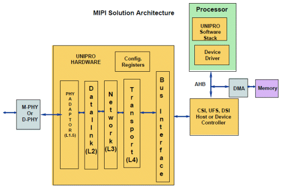
Figure 2: MIPI Standard Architecture with UniPro
The following sections discuss specific products and explain the logic blocks within them
PHY
The PHY and UniPro products are the basis for the bus connections and are common to the different standards controllers.
Arasan offers the D-PHY and M-PHY as well as the UniPro link layer. The D-PHY is a synchronous, point-to-point connection of up to four lanes. It operates in either high-speed or low-power modes and supports up to 1 G Bit of bandwidth.
The M-PHY products are Type 1 or Type 2 (with DigRF). Both are current to the specification with analog line transmit and receive sides in analog. Behind the analog is the digital side with state monitors and drivers.
Customers using the D-PHY can upgrade to an M-PHY when the standards they are using adopt that technology.
UniPro
UniPro has been adopted as the standard Link layer for UFS and DSI controllers and may be adopted for use with CSI as well. The UniPro core includes a PHY interface as well as the Data Link, Network, Transport layers and a bus interface. Customers select from among several bus interfaces and there is a DMA engine available for hardware-controlled transfers.
The UniPro product includes a software stack that runs on the system processor and controls the flow of data through the UniPro digital logic. The software has APIs that initialize, configure, control data flow and perform other tasks. The stack includes a scheduler that maintains connection-specific queues and delivers QOS for them. UniPro is responsible for both data layer and end-to-end flow control.
The UniPro controller implements several layers of hardware processing of segmented messages between Host and Device. The layers in the controller include the L1.5 PHY Interface and the L2 Data link. The PHY interface controls the flow of DLL control and data symbols from the PHY. The interface also manages power.
The L2 layer adds or strips a header and a trailer and calculates and appends the CRC to the segment. It assembles and disassembles frames. The L2 performs flow control using the local FIFO and performs CRC generation and checking.
The L3 Network layer inserts or strips its header consisting of the C-Port ID. It supports both the TC0 and TC1 traffic classes.
The L4 Transport layer inserts or strips the device ID header information. The L4 also communicates with L2 as to the amount of data to transfer effecting end-to-end flow control as well as performing error handling.
Camera Serial Interface (CSI)
The CSI Receiver and Transmit controller cores complement each other in capturing, processing, displaying and controlling camera data. A sample CSI-2 system is shown in Figure 3.
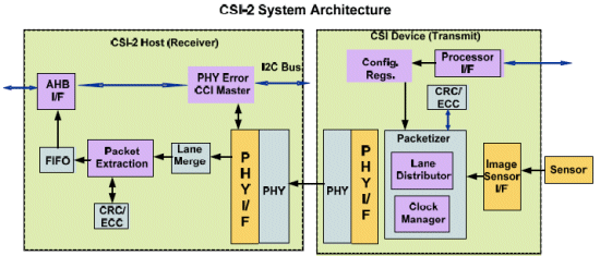
Figure 3: CSI System Architecture
The Transmit (Device) core sends camera data over the bus and the Receiver (Host) processes it for display. The core includes a clock and power management unit to generate quadrate clocks.
The Packetizer has the land distributor and clock manager blocks. The lane distributor encapsulates packets with identifier wrappers, a header, footer and a payload that depends on the image format. The lane distributor also distributes data among the one to four data lanes.
The PHY interface drives the data lanes of the PHY. The CRC and ECC generators append their values to the data payload.
The processor interface links the core to the external signal processor that generates frame and line information along with pixel data and payload size. The virtual channel number and the data type to which the frame is to be sent are received as part of the packet interface signaling.
The receiver core supports up to four data lanes as programmed by the AHB processor. The lane merger aggregates data from the lanes into an eight-bit bus. The receiver detects whether the operation mode is high-speed or low-power by monitoring the state of the PHY to see whether it is operating in ULPS mode, low power mode and high speed mode.
The detection logic includes a traffic monitor the initialization counter at low-power mode and packet reception timeout counters at high-speed mode are placed in this block to verify remaining in the current operating mode.
The packet extractor removes the wrapper from the packet data bytes. The packet header, short packets, packet footer and payload data are extracted from the data stream and fed to the appropriate blocks for essential processing of the data.
The ECC corrector block corrects data in the packet header and short packets for one-bit error correction or two-bit detection and the status stored in the error correction status register.
The ECC generator operates on the packet header and for short packets and forwards the generated value to the ECC corrector block. CRC Checker generates the checksum for the payload data and registers the information in the register set for further processing of the payload.
The current CSI-2 versions of the cores will be upgraded to version CSI-3 when the specification is released.
Display Serial Interface (DSI)
The DSI Receiver and Transmitter pair performs transfers of display data. The data is transferred over a serial bus of up to four lanes.
The DSI cores specify the interface between a host processor and a display module. The system consists of a DSI Host (transmitter) and a DSI Device (receiver). The cores are built on existing MIPI Alliance standards by adopting pixel formats, controlling pins and command set specified in DPI-2, DBI-2 and DCS standards.
The cores support the four types of display architecture specified in the standard, namely Types1-4. The types are distinguished by the hardware and software resources used in the rendering of images.
The DSI specification provides for high-speed signaling that operates at 1000Mbs and a lowpower signaling 10Mbs. The mode is set at start up. The lanes switch between high and low power modes depending on the desired data transfer type.
High-speed data transfer is unidirectional while low-speed transfers can be unidirectional or bidirectional. The data are processed on the Host processor and forwarded through the Host and the Device to be rendered on a display on the system side of the Device. A DSI system is shown in Figure 4.
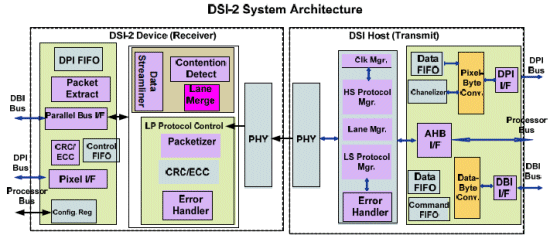
Figure 4: DSI System Architecture
The Host DPI interface generates control signals on receipt of a short packet. The DPI controls are forwarded to the Pixel interface to generate frame timing, blanking time and line timing.
The DBI interface links the core to an external display device. Controls are derived from the command FIFO along with the accompanied parameters. If the command is a DCS long write, for example, then the command stored in the first location of the Data FIFO is sent in the DBI interface and the accompanied data as listed in the word count field of the control FIFO are passed on to the DBI interface for the data phase.
The pixel-to-byte converter makes pixel data into byte format and stores it in the data FIFO. Data width to byte converter: Converts the data from different widths on the DBI interface to byte format and stores in Data FIFO. The contents of the FIFO are formed into packets for forwarding across the serial bus.
High Speed Protocol Handler manages data transfers depending on the packet information in the control FIFO. The control may direct the formation of short or normal packets. If the control requires a long packet, then the Data FIFO content is padded as described by the control FIFO.
The Channelizer contains a state machine that grants DBI transfers whenever the horizontal or vertical synchronizers transition or RGB data is not transmitted by the DPI stream. The BLLP timings are fully occupied for DBI transfer or Generic transfer or DCS commands transfer via DSI packets.
The Error Handler has an ECC/CRC generator block to generate and check ECC and CRC on packet data.
On the Device side the Lane Manager distributes byte data among the serial lanes. The number of data lanes is programmed via registers in AHB target interface. It also drives the clock and data lanes of the PHY. The lane merger is clocked on the incoming side at speeds varying from 40MHZ to 500MHz. A receive byte clock which is one quarter of the high-speed data clock is used for interfacing with the D-PHY control signals.
The DPI interface generates control signals once the short packets carrying DPI events are signaled to the pixel interface. The controls include frame timing, blanking time and line timing information. The data bytes that are sent via long data packets are directed to a data FIFO and are streamlined for further processing. Based on the header information that accompanies each long packet the data bytes are again converted to pixels and sent to the pixel interface.
The DBI interface links the core to external display device. The control FIFO contains the DCS/ Generic commands along with the command parameters. If the command is a DCS long write, then the command stored in the first location of the data FIFO is sent to the DBI interface and the accompanied word count field of the control FIFO is passed on to the DBI interface for the data phase.
The lane merge block concatenates the lane serial streams data into a single stream. The receiver has logic to detect the different states of the PHY like ULPS state and high-speed mode.
The high-speed streamer merges incoming serial data into a byte stream to be passed to the packet extractor, CRC and ECC units.
The Low Speed Protocol Handler removes the wrapper and extracts data bytes from packets.
The header, footer and payload data are extracted from the data stream and fed to the ECC and CRC checkers. Reverse data reception at low speed and bus turnaround timing are also performed by this block.
The Error Handler monitors contention errors that occur in low-power operation. The handler also has timers to monitor high-speed transmit timeout, low-speed reception, turn-around Timeouts, fault mode recovery counters and device reset timers for contention recovery. Protocol errors are passed on to processor as interrupts
The core has packet transmission timeout counters that work during low-power mode and packet reception timeout counters that operate during high-speed mode are used to monitor the DSI traffic to ensure that the receive logic is in the proper state for the operative mode.
The extractor block removes the wrapper and segregates data bytes from the DSI packet format. Packet header, short packet, packet footer, payload data are split up from the data stream and are fed to the appropriate blocks for processing. The high-speed extractor operates on fast data streams while the low power extractor operates on one clock the video data is buffered in the DPI FIFO.
The data is sent in packets through a FIFO and are streamlined for further processing. Based on the header information that accompanies each long packet the data bytes are again converted to pixels and sent to the Pixel interface.
Commands and data received at high-speed as well as at low-power operation are gathered in the DBI control and data FIFOs.
The Low Power Protocol handler performs packet formation, ECC and CRC generation, and error responses. The low-power Protocol handler is comprised of the Packetizer, ECC generator, CRC generator and an error and response handler.
The Packetizer operates during low-power clock transfers sending trigger messages, acknowledgment packets and generic/DCS mode read responses in long or short packets.
The low-power ECC and CRC generators create the packet CRC, correct single bit errors and detects two-bit errors in the data stream and packet header. The error status register stores the error correction status.
Errors in the DSI stream such as EOT error, SOT sync error, escape mode error, entry command error, LP transmission error or false controller are sent back to the host by the response handler in short packet form and low power mode.
The errors are sent over the AHB to the processor as interrupts. For irrecoverable errors such as multi-bit ECC, packet length errors the DSI-RX device controller stops processing further data and forces the D-PHY to go to stop state and resumes recording of the events for the next DSI high speed transfer.
For DCS Read commands, the number of data bytes collected for this DBI read operation is based on the maximum return packet size register settings. Similar is the case with generic Read too.
The AHB interface houses the DSI operational registers and is the processor access port. The processor programs the configuration register and passes interrupts to the processor.
Universal File System (UFS)
The UFS system, Figure 5, consists of a Host and Device controllers. The Host configures the Host registers as well as the Device Controller and Device Logical Units (LU). Each LU contains mappings to locations in data storage. The LUs can process commands to perform data transfers.
The UFS Host accepts commands and data from the host processor under the control of the application and UFS device driver.
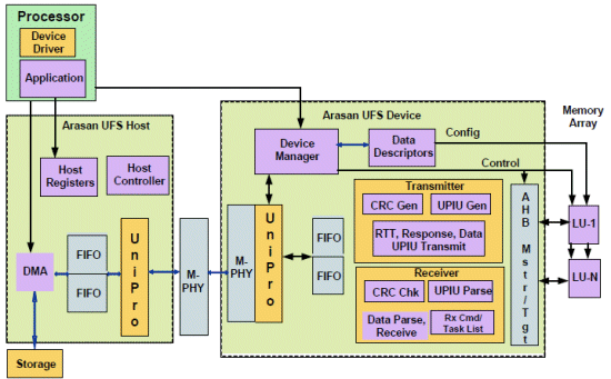
Figure 5: UFS Standard System Architecture
SLIMbus
The SLIMbus is a low-power, two-wire, multi-drop TDM bus supporting connection of a wide variety of audio and digital specifications for mobile applications. Arasan offers both Host and Device SLIMbus cores as shown in Figure 6 that are fully compliant with the SLIMbus specification.
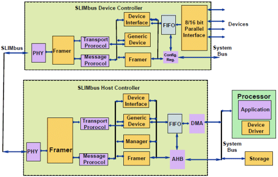
Figure 6: SLIMbus Host and Device System Architecture
The bus is designed for a throughput of up to 28.8 Mbps and supports multiple devices each having up to 64 I/O ports. The ports are programmable and support isochronous and extended asynchronous transport protocols. The manager performs configuration and controlling functions by sending control messages via the shared message channel. It is also responsible for assigning logical addresses to any device that is authorized to communicate on the bus.
The framer is responsible for driving the clock signals and generating the SLIMbus frames. The SLIMbus Host also supports a special clock gear function to dynamically change clock frequencies to optimize bus power consumption.
Designed specifically for applications such as mobile phones, portable handheld media players, and mobile terminals, the SLIMbus provides universal connectivity between the applications processor and low-throughput devices in the system such as microphones, speakers, keypads, ringers, and Bluetooth devices.
The SLIMbus Host Controller IP core utilizes a master/slave AHB or alternative system bus.
SLIMbus Stack
The Stack is a software product Arasan offers that supports the Host and Device controllers. The Stack supports SLIMbus systems running on various operating systems and hardware platforms. The Stack supports systems with multiple hosts and devices using Linux and other operation systems. It can also be ported to different hardware platforms.
The Stack consists of the General Application Interface layer, SLIMbus Driver, and Host Controller Driver. Client applications interface with the General API layer directly or through a Device Class Driver layer.
The SLIMbus Driver implements protocols such as isochronous and asynchronous data transfer, enumeration, and message handling. It also supports functionalities specific to the Arasan SLIMbus Host and SLIMbus Device IP cores. The Host Controller Driver is a hardware dependent layer. It is designed to operate on different hardware platforms.
The drives comes with a well defined API package includes commonly used functions for initialization, configuration, data transfer, power management, and interrupt handling. To facilitate development of new products, an optional Device Class Driver is also available. These device classes include SPI, I2C, I2S, ADC, DAC, UART, BT, and Flash.
SLIMbus Analyzer
The analyzer is a development tool for systems using SLIMbus Hosts and Devices. The protocol analyzer provides the mobile industry a versatile tool to assist in the development and debugging of SLIMbus® products. It can be used by system developers, system integrators, software developers and system quality analysts to debug as well as validate their products during the product lifecycle.
The analyzer, shown in Figure 7, is a hardware and software system. The software runs on a PC which is connected by an Ethernet cable to the hardware. The hardware is a box with two cards. One card generates SLIMbus traffic under the direction of the operator. The traffic analyzer card
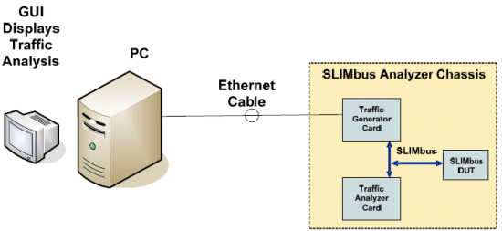
Figure 7: SLIMbus Analyzer Hardware System
Arasan’s SLIMbus protocol analyzer includes an aesthetically designed and intuitive GUI. The GUI allows you to configure the hardware and software parameters of the system. The Grid View display mode shows information on data packets, can be used to start or stop their capture, perform sorting, searching, filtering analysis and also save data to a file for post processing. The analyzer can generate reports as well as display dynamic run-time charts for capture statistics.
Users create traffic on the GUI. The traffic is then forwarded over the Ethernet cable to the Traffic Generator Card. The traffic may be processed by a DUT SLIMbus card and it is analyzed by the Traffic Analyzer Card. The results are forwarded back to the PC for viewing.
The analyzer provides complete details on the activities going on the bus such as the sources and destinations of transfers, transfer sizes data by which device on the bus, the management information being exchanged on the SLIMbus.
The analyzer provides expert analysis using a set of graphical charts to depict the various parameters of traffic on the bus, devices available on the bus, active and inactive devices and data channels.
The tool monitors the SLIMbus® and instantly identifies problems. It permits the designers to set event triggers and alarms when a condition is encountered. Triggers are especially useful during long regressions when the system is not monitored
Low Latency Interface (LLI)
The Arasan LLI IP product is developed as the specification proceeds and will be released coincident to the specification. The LLI specification defines an interface for sharing a DRAM memory between two devices such as a processor and co-processor. The shared memory will reduces system costs.
Another benefit of LLI is the ability to connect companion processors to exchange information without software intervention. Such exchanges enable remote configuration and memory mapped transfers among multiple devices as if they were one.
The LLI specification defines several logical layers as follows:
- Transaction layer - Defines memory mapped read/write transactions and signals between devices.
- Data link layer - Provides several independent virtual channels between the two devices
- PHY adapter layer - Provides an interface to the physical media
- Power management - Optimizes power consumption and defines power states
Summary
The hand-held product market richly rewards those who can quickly offer products with the latest and most powerful standards. Customers using IP products that implement those standards should seek a vendor who can quickly bring their design to market by providing a complete solution to all their MIPI standards requirements.
Arasan Chip Systems Inc.
2010 N. First Street, Suite 510
San Jose, CA 95131
Phone: 408‐282‐1600
Fax: 408‐282‐7800
Email: sales@arasan.com
Data Sheets Link: http://www.arasan.com/datasheets/login.php
For a complete directory of Arasan products, please visit: www.arasan.com
Related Semiconductor IP
- UFS 5.0 Host Controller IP
- PDM Receiver/PDM-to-PCM Converter
- Voltage and Temperature Sensor with integrated ADC - GlobalFoundries® 22FDX®
- 8MHz / 40MHz Pierce Oscillator - X-FAB XT018-0.18µm
- UCIe RX Interface
Related Articles
- Improving Inter Integrated Circuits - From Sensor Hubs to Platform Management Solutions
- MPEG Standards -> Latest MPEG efforts: solutions or confusion?
- MEMS -> Advances, pitfalls seen with MEMS solutions
- SoCs lend momentum to design-for-test solutions
Latest Articles
- Enabling RISC-V Vector Code Generation in MLIR through Custom xDSL Lowerings
- A Scalable Open-Source QEC System with Sub-Microsecond Decoding-Feedback Latency
- SNAP-V: A RISC-V SoC with Configurable Neuromorphic Acceleration for Small-Scale Spiking Neural Networks
- An FPGA Implementation of Displacement Vector Search for Intra Pattern Copy in JPEG XS
- A Persistent-State Dataflow Accelerator for Memory-Bound Linear Attention Decode on FPGA