Verification Planning for Core based Designs
Infineon Technologies Asia Pacific Pte Ltd
Singapore
Abstract:
Verification planning is an important and integral part of verification, irrespective of the size of the system. About 70% of the design cycle time is spent on verification; with proper verification planning some of the issues faced during the later phases of design can be addressed earlier. For SOC’s it is observed that most of the peripherals are reused from the previous design step with some modifications done on the feature set. Verification reuse methodology is very critical for these systems. In this paper we will be discussing about the importance and completeness of verification planning in order to achieve the verification requirements and reuse techniques adapted during the planning phase to enhance reuse between different cores based designs.
Introduction
Verification planning can be described as a set of goals that needs to be verified. With increasing complexity it is very difficult to check the completeness of the verification planning, hence a verification plan can be said to be complete if it satisfies the objectives specified in the requirements and system objectives. Verification planning should be independent of the tools used. This gives the flexibility to decide the right tool to achieve the verification goals. Normally a verification plan would consists of 1) Functional requirements 2) Design requirements 3) Defining coverage goals 4) Embedded firmware requirements apart from these the verification plan should also focus on reuse for core based designs. A typical SOC could consist of Core, Communication peripherals, DMA, Memory controller (interface to external memory such as SDRAM, Burst Flash ….).
Some of the Basic steps for deriving the Verification plan
Analyzing the Specification
The specification is supposed to capture the requirements and the intended behavior of the design. Our objective from specification analysis is to extract the required features of the design. While analyzing the specification it is necessary to split it into functional and design requirements.
Functional requirements: - Here Functional requirements can be defined as the behavior required by the system. How different is functional requirement from design requirement? Functional requirement would be looking into the practical usage of the chip and trying to create the scenarios for such an application. Some examples are
-
The practical usage would be to use the communication module for display while the other peripherals are involved in data transfer.
-
Plugging out the debugger while the system is partially reset.
-
Power saving features invoked while exercising the interrupts.
These requirements are then translated to stress tests on system level.
Design requirements: - Verification planning for design requirements is to check the implementation against the specification. In this stage, we do not stress on the practical usage but on the actual implementation of the design. These requirements can be translated into directed, directed random requirements or stress tests for peripherals.
For a complex design, verifying the complete design requirements is a time consuming and tedious task. For verifying the design requirements, bottom-up verification approach can be adapted to reduce the effort spent on SOC level. The Design requirements need to be split into system-specific requirements and peripheral specific. The peripheral-specific requirements are those which can be verified in module level.
Examples of peripheral-specific requirements are
-
Verifying all possible baudrate for a UART.
-
Verifying communication interface for slowest and the fastest clock speeds.
System specific requirements focus more on system level issues. Some of the system-specific blocks such as reset generation unit, clock generation unit can be completely verified only on system level.
Examples of system-specific requirements are
-
Verifying the system is properly reset for the different types of reset.
-
Verifying the system for different power saving modes
-
Verifying the interconnectivity of clock.
-
Verifying the connectivity to pads, interrupts, debug interfaces.
With this approach, the peripheral is verified completely in the module level. The SOC level verification could then focus more on top-level issues such as interconnectivity, interrupt system behavior (response of interrupt for that peripheral), bus interfaces, I/O interfaces. The system level verification could focus more on system level issues and speed up the overall verification process.
Identifying Coverage goals
Coverage plays an important role in SOC verification. It gives a detail breakdown on issues tested against those untested. It is good to have a complete coverage metric for all the peripherals, but this would mean additional overhead for simulators which would slow down the simulation speed drastically. There has always been a compromise for coverage against the simulation speed. Hence it becomes necessary to understand the complexity of the design before identifying the coverage points. The intended coverage could be achieved by assertions or by coverage metric. Either way the definition of coverage points plays a very important role. For SOC verification it would be good to have interconnectivity coverage, coverage for interrupts, system-specific behavior such as power saving features, recovery sequences, reset and clock (power saving features), and system buses.
Some examples for coverage are
-
Coverage of reset path for the entire system. It is necessary to check that all the peripherals are reset properly.
-
Coverage of various boot options.
The detail functional coverage for the peripheral could be covered in independent module level verification. Identifying coverage points is an iterative process involving module designer and concept engineers.
Embedded Firmware requirements
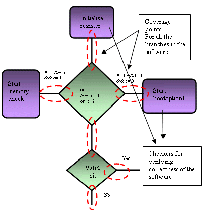
What is an embedded Firmware? Well, an embedded firmware can be described as a piece of software embedded into the ROM/EPROM which would initialize the chip into a defined state on reset. This piece of software could contain Startup sequences, bootstrap loaders, memory test routines, tests for production etc. It can be seen that this software is very complex and the corresponding verification is a complex task. Unlike the verification of peripherals, firmware verification is restricted to SOC level which further increases the complexity of verification. So how do we ensure this piece of software works? For firmware verification, it is necessary to have a good coverage metric. During the verification planning phase, we need to identify all the coverage points with iterative process of review from the members involved in the development of concept and firmware. Normally the firmware verification plan is a list of coverage items that needs to be addressed in the process.

Fig 1. Defining coverage points for Firmware
From Fig 1, it can be seen that it is necessary to have good branch coverage metric for firmware.
In order to achieve a good coverage metrics it is necessary to know the firmware, unlike the module verification where the DUT is treated as a black box, for firmware it is necessary for the verification engineer to know the flow of the firmware. Fig 1. gives an example of the flow of the firmware code. Normally the firmware which consists of software is compiled and translated into memory dump files. These memory dump files are read by the memory during the startup of the simulation. It is difficult to get the code coverage for a memory dump, hence PC is translated into coverage points.
An example of Firmware code
MEM(status) = software_boot;
Software_start();
else if (HWCFG = “011”) then
MEM(status) = ext_boot;
Ext_start();
else
MEM(status) = int_boot;
Internal_boot();
End if;
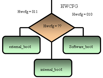
The firmware code can then be translated to a flow chart which gives the verification engineer an overview of the software flow.

Fig 2. Flowchart of the software
The conditional statement and status information are then translated into checkers, while the branching information is taken from the translated PC. With this we can get a complete coverage for the software code.
Defining Reuse
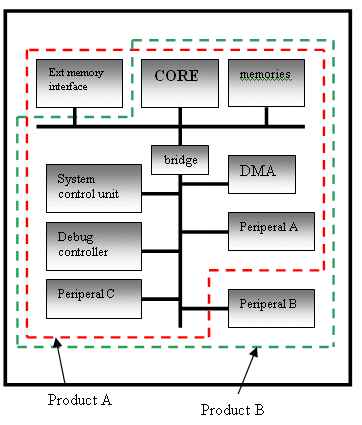
Having defined the above basic steps for verification planning, we shall now focus on how to achieve verification reuse with proper planning. The concept of reuse is simple in theory but it is quite tough to achieve. Achieving good reuse is a team effort; concept and design teams have to work out a proper strategy for reuse while the verification team need to workout on the reuse methods for the verification environment. Let us look at achieving reuse for a family of products

Fig 3. Overview of the product family
Product A and Product B are similar in architecture with variations in peripherals and memories used.
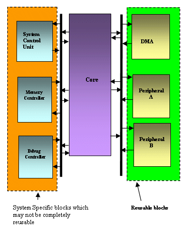
So how do we plan reuse? Planning reuse is not a straightforward approach. It is an iterative process where in you need to understand the possible changes required. It is not possible to achieve good reuse for dynamic modules i.e. those modules where most of the features are changed for every design step; reuse can be planned for those modules where the degree of changes is minor. Before planning reuse, it is necessary to take a deeper look into the architecture of the product. It is necessary to segregate the blocks where higher degree of reuse can be achieved against those where reuse is practically not possible. Fig 4. gives an overview of the reusable components. On defining the reusable components the verification plan has to be separated such that the non reusable components are segregated.
For example
1. Verifying the connectivity of interrupt lines of peripheral A can be in common for Product A and Product B.
If the interconnectivity for Peripheral A with DMA differs in Product A and Product B the verification planning must incorporate such difference.

Fig 4. A complex SOC design with reusable and non-reusable components
Some of the essentials for planning reuse are:
-
The tests should be generic and I/O definition, register definition should be separate i.e. must be handled in different header files which could be modified based on SOC requirement.
-
The verification plan must separate reusable and non-reusable features to separate testcases for enhancing reuse. For example, if it is known that Peripheral A is normally reused between SOCs with major changes in I/O mapping, then the verification plan should separate the verification of I/O mapping with a separate testcase.
-
While planning verification requirements, it is also necessary to identify tests that would be used for post-silicon analysis; this would reduce the effort of redeveloping testcases for post-silicon analysis.
-
During verification planning, it is necessary to ensure that the effort of verification is not duplicated much. For example, if interconnectivity to interrupts is part of peripheral A in SOC verification then interconnectivity for these interrupts can be excluded for interrupt controller SOC verification.
-
System stress tests and directed tests (peripheral interconnectivity tests) have to be separated as the possibility of reuse for directed tests are more compared to stress tests for SOC.
Verification plan gives an early estimate on effort, resource required, reuse percentage and coverage goals. Verification closure is an iterative process where the plan is measured against the implementation and coverage goals. Verification reuse can be achieved with proper planning, reusable verification environment and proper documentation.
References
1. “How to improve verification planning” by Steve Brown, Cadence Design system, Inc.
2. “Verification Planning to Fuctional Closure of Processor based SOC’s” by Andrew Pizzali, Cadence Design System, Inc., DesignCon 2006
3. “Reusable Verification Environment for Core based Designs" by Teng-Peow Ng, Anjali Vishwanath, Rizal Prasetyokusuma & Ranga Kadambi, Infineon Technologies Asia Pacific Pte Ltd, IP/SoC 2004
Glossaries
DMA Direct memory Access controller
SOC System on chip
HWCFG Hardware configuration
Related Semiconductor IP
- oFEC Encoder and Decoder
- NPU IP Core for Edge
- NPU IP Core for Mobile
- NPU IP Core for Data Center
- NPU IP Core for Automotive
Related White Papers
- An IP core based approach to the on-chip management of heterogeneous SoCs
- Reusable Verification Environment for Core based Designs
- Low Power Design Methodology for Core based ASSP
- Design and implementation of Parallel and Pipelinined Distributive Arithmetic based Discrete Wavelet Transform IP core
Latest White Papers
- Customizing a Large Language Model for VHDL Design of High-Performance Microprocessors
- CFET Beyond 3 nm: SRAM Reliability under Design-Time and Run-Time Variability
- Boosting RISC-V SoC performance for AI and ML applications
- e-GPU: An Open-Source and Configurable RISC-V Graphic Processing Unit for TinyAI Applications
- How to design secure SoCs, Part II: Key Management