Design and implementation of Parallel and Pipelinined Distributive Arithmetic based Discrete Wavelet Transform IP core
Asst. Professor MSRSAS
VLSI System Design Center
M.S.Ramaiah School of Advanced Studies, Bangalore
ABSTRACT
The Discrete Wavelet Transform (DWT) has gained the reputation of being a very effective signal analysis tool for many practical applications. This paper presents an approach towards VLSI implementation of the Discrete Wavelet Transform for image compression. The design follows the JPEG2000 standard and can be used for both lossy and lossless compression. In Discrete Wavelet transform, the filter implementation plays the key role. The poly phase structure is proposed for the filter implementation, which uses the Distributive Arithmetic (DA) technique. The implementation of DA based DWT IP core in ASIC (Application Specific Integrated Circuit) exploits the lookup table-based architecture, which is popular in FPGA (Field Programmable Gate Array) implementations. To exploit the available resources on FPGAs, a new technique, which incorporates pipelining and parallel processing of the input samples, is proposed, with this architecture the speed (throughput) of the design increases by 25%. The intermediate coefficients obtained are efficiently stored in a memory and accessed for efficient memory utilization on FPGAs. The design is targeted on Xilinx spartanIIE, and the ASIC design of the same is carried out.
This work is carried out in M S Ramaiah School of Advanced Studies, Bangalore in partial fulfillment of requirements for the award of M.Sc (Engg) in VLSI System Design degree from Coventry University, U.K
1.INTRODUCTION
The discrete wavelet transform (DWT) is being increasingly used for image coding. This is because the DWT can decompose the signals into different sub-bands with both time and frequency information [1] and facilitate to arrive a high compression ratio and it supports features like progressive image transmission (by quality, by resolution), ease of compressed image manipulation, region of interest coding. The JPEG2000 also adopts the DWT into its standard. Recently several VLSI architectures have been proposed to realize single chip designs for DWT. Traditionally, such algorithms are implemented using programmable DSP chips for low-rate applications, or VLSI application specific integrated circuits (ASICs) for higher rates.
In wavelet transforms, we divide the original signal into frequency resolution and time resolution contents. For this purpose, a cutting window will be used. This window is known as “Mother Wavelet”. The problem here is that cutting the signal corresponds to a convolution between the signal and the cutting window. The signal will convolve with the specified filter coefficients and gives the required frequency information. The decomposition of the image using 2-level DWT is as shown in figure.1.
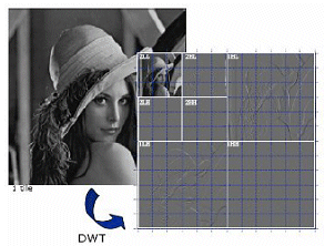
Figure.1. Decomposition of Image [1]
To perform the convolution we require a fast multiplier, which makes the operations efficiently. Because filter coefficients remain constant during the entire duration of a transform, constant coefficient multipliers (CCMs) were considered for the design. In this thesis, Distributed Arithmetic based multiplier is used for this purpose. Distributed arithmetic is a bit level rearrangement of a multiply accumulate to hide the multiplications. It is a powerful technique for reducing the size of a parallel hardware multiply-accumulate.
The paper is organized as follows; Section 2 describes the brief concept of the traditional DWT and convolution-based filter architecture specified in JPEG2000 standard. In Section 3, a detailed analysis of the distributive arithmetic algorithms and filter architecture will be addressed. Finally, ASIC implementation and the conclusions are presented in Section 4 and section 5. The references are mentioned in Section 6.
2. CONVOLUTION BASED DISCRETE WAVELET TRANSFORM
The traditional DWT can be realized by convolution-based implementation [2] [3]. In the forward transform, the input sequences are down sampling and filtered by the low-pass filters and high-pass filters to obtain the low-pass and high-pass DWT coefficients, and . The equations may be written as follows:

The poly-phase structure for the convolution based DWT is as shown in the Figure.2. The poly-phase form takes advantage of splitting the input signal into odd and even samples (which automatically decimates the input by 2), similarly, the filter coefficients are also split into even and odd components so that Xeven convolves with G0,even of the filter and Xodd convolves with G0,odd of the filter. The two phases are added together in the end to produce the low pass output. Similar method is applied to the high pass filter where the high pass filter is split into even and odd phases H0, even and H0, odd.

Figure.2. Poly-phase high pass filter bank [2]
The FDWT can be performed on a signal using different types of filters such as db9, db7, db4 or Haar. The Forward transform can be done in two ways, such as matrix multiply method and linear equations. In the FDWT, each step calculates a set of wavelet averages (approximation or smooth values) and a set of details. If a data set s0, s1 ... sN-1 contains N elements, there will be N/2 averages and N/2 detail values. The averages are stored in the upper half and the details are stored in the lower half of the N element array. In this paper, Daubechies 9/7 filter coefficients are considered. The filter coefficients are given in table.1. [4][5]
Table.1. Daubechies 9/7-tap filter coefficients
| TAPS | LOW PASS FILTER | TAPS | HIGH PASS FILTER |
| 4 | 0.6029490183263579 | 3 | 1.1115087052456994 |
| 3,5 | 0.2668641184428723 | 2,4 | -0.5912717631142470 |
| 2,6 | -0.078223266528987 | 1,5 | -0.0575435262284995 |
| 1,7 | -0.016864118442874 | 0,6 | 0.09127176311424948 |
| 0,8 | 0.02674875741080976 | |
By using the filter structure proposed, the 3-level image compression is as shown in figure.3.
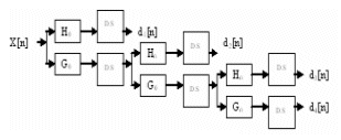
Figure.3. Image Decomposition [1]
3. DISTRIBUTIVE ARITHMETIC BASED ARCHITECTURE
In this section, we first outline how to perform multiplication by using memory-based architecture. Following this, we briefly explain architecture for DWT filter bank. Using this we show complete design for block based DWT.
In computing the DCT, DFT and DWT multipliers are the fundamental computing elements. Since these multipliers consume significant area, the number of multipliers and adders that can be employed on a chip is limited. The memory-based approach provides an efficient way to replace multipliers by small ROM tables such that the DWT filter can attain high computing speeds with a small silicon area.
Traditionally, multiplication is performed using logic elements such as adders, registers etc. [6] However, multiplication of two n-bit input variables can be performed by a ROM table of size of 22n entries. Each entry stores the pre-computed result of a multiplication (See Figure.4). The speed of the ROM table lookup is faster than that of hardware multiplication if the look-up table is stored in the on-chip memory. In general 22n-word ROM table is too large to be practical. In DWT, one of the input variables in the multiplier can be fixed. Therefore, a multiplier can be realized by 2n entries of ROM as shown in Figure.4.
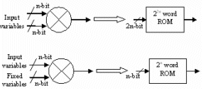
Figure.4. ROM table approach for multiplication. [6]
3.1 Design of filters
The computational modules of DWT consist of filters, and as defined in previous section. [8] The transfer function of these filters can be represented as,

The DWT filters consist of filter coefficients g (i) and delays z-i. The DWT coefficients are generated after applying the high-pass and the low-pass filter. Assume that the size of input variables is n bits. If we multiply the l input variables with the filter coefficients in parallel, l n-bit multipliers and {l-1}2n-bit adders are needed.
In the proposed memory based architecture the multiplications are performed using ROM tables. The size of the ROM table needed to implement a filter with n input variables is 2n. The table consists of all the possible combinations of input. The table with three filter coefficients is as shown in the Table.2.[9]
Table.2. Look-up table
| Address | Content | Address | Content |
| 000 | 0 | 100 | C2 |
| 001 | C0 | 101 | C2+C0 |
| 010 | C1 | 110 | C2+C1 |
| 011 | C0 +C1 | 111 | C2+C1+C0 |
To access the look-up table, we have the same number of registers as filter coefficients. The input x[n] will enter into the serial shift register which has to access the look-up table. When the next input comes into first register, the old value will be pushed into the next register. In the same way, when next values come into registers, the old values will go off from the registers.
Now, to get the address from the input values, we consider the bit positions and get the values of inputs by that bit position. For example, if we want to get the first address, we have to consider the LSBs of all serial registers. By this address we will get the first position value. In the same manner, we have to get all bit position addresses and get the corresponding values from the look-up table. While adding, we have to shift the values by the bit position value and give them to adder. Finally, we have the result, which is the convolution of the filter coefficients and the inputs. The accessing of look-up table is as shown in the figure.5.
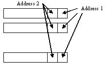
Figure.5. Accessing ROM table
The same architecture will be used for the both high-pass and low-pass filters. If the input is 8-bit length, then we require 8 clock cycles to get the convolved value. In computing the wavelet coefficients the filter operations are specified using floating-point arithmetic. However, integer arithmetic is used in practice. Thus, the filter coefficients are truncated. This truncation reduces the accuracy of the computed coefficients and hence affects the reconstructed image quality. By using a wide length multiplier, we can reduce the truncation error and can potentially improve the image quality.
From Table.1, it is clear that the filter coefficients are in fractional form. To represent them in binary form, number of the representation bits will increase. So, the number of computations will increase. So, we have to round off them to decimal values. For, this we have to multiply each coefficient with a known higher decimal value. In this paper, decimal number 256 is considered. At the final stage, we have to divide the results with the same 256.
To speed up the process we can go for the parallel implementation of the Distributive Arithmetic (DA). The structure is as shown in the figure.6. In parallel implementation, we divide the input data into even samples and the odd samples based on their position. Even we can split the filter coefficients into even and odd samples. So, the even samples convolve with the even and odd filter coefficients and at the same time the odd samples also convolve with the same coefficients. So, by the same time we are getting the result for both even and odd samples of input.
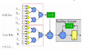
Figure.6. Parallel implementation of DA technique. [3]
4. ASIC IMPLEMENTATION
Using bottom-up design flow did the coding. i.e., the individual components were designed by using behavioral coding and finally the individual blocks were connected by using the structural description.
The design was implemented on SPARTAN-2E FPGA board with the 32x32 image. For the implementation the image was stored in a ROM and mapped on to the FPGA. The DWT code was mapped on to another FPGA and interfaced together. The results were observed on the LEDs. The same code was simulated in ModelSim simulator.
After simulating the designs extensively, they were synthesized using the Synopsys Design -Compiler with TSMC’s 0.13-micron CMOS standard cell library at 125 MHz frequency. The designs were optimized for delay with a maximum output capacitance of 0.1, an operating voltage of 1.2 V, and a temperature of 250 C.
The synthesized code was compared with the reference design and find that both are same. For this purpose, Synopsys Formality has been used. The tool take some reference points in implemented design and compare with the reference design.
Static timing analysis was carried out using Primetime. In Primetime block level timing analysis is carried out for the same design compiler constraints. The timing analysis was done two times, before and after the layout. In pre-layout timing analysis, wire load models were used to calculate the delays. In Post global route timing analysis, the original parasitic values were considered. Finally, the placement and routing is carried out in the Synopsys Astro. In the process, the placement is carried out manually; timing analysis was done for the placed design. The final placed and routed design is as shown in figure 7.
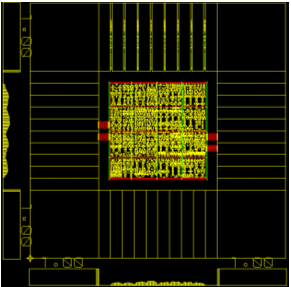
Figure.7. Placed and Routed design from Astro
5. CONCLUSIONS
The Discrete Wavelet Transform provides a multi-resolution representation of images. The transform has been implemented using filter banks. For the design, based on the constraints the area, power and timing performance were obtained. Based on the application and the constraints imposed, the appropriate architecture can be chosen. For the Daubechies 9/7-biorthogonal filter, the poly-phase architecture, with DA technique was implemented. It is seen that, in applications, which require low area, power consumption, and high throughput, e.g., real-time applications, the poly-phase with DA architecture is more suitable. The biorthogonal wavelets, with different number of coefficients in the low pass and high pass filters, increase the number of operations and the complexity of the design, but they have better SNR than the orthogonal filters. The DWT IP core was designed by using Synopsys ASIC design flow. First, the code was written in VHDL and implemented on the FPGA using a 32x32 random image. Then, the code was taken through the ASIC design flow. For the ASIC design flow, a 8x8 memory considered to store the image. This architecture enables fast computation of DWT with parallel processing. It has low memory requirements and consumes low power. By using the same concepts, which are mentioned above, are useful in designing the Inverse Discrete Wavelet Transform (IDWT).
6. REFERENCES
1. David S. Taubman, Michael W. Marcellin – JPEG 2000 – Image compression, fundamentals, standards and practice”, Kluwer academic publishers, second printing – 2002.
2. G. Knowles, “VLSI Architecture for the Discrete Wavelet Transform,” Electronics Letters, vol.26, pp. 1184-1185, 1990.
3. M, Vishwanath, R. M. Owens, and M. J. Irwin, “VLSI Architectures for the Discrete Wavelet Transform,” IEEE Trans. Circuits And Systems II, vol. 42, no. 5, pp. 305-316, May. 1995.
4. Charilaos Christopoulos, Athanassios Skodras, and Touradj Ebrahimi - "THE JPEG2000 STILL IMAGE CODING SYSTEM - AN OVERVIEW", Published in IEEE Transactions on Consumer Electronics, Vol. 46, No. 4, pp. 1103-1127, November 2000.
5. Andraka consulting group,Inc – “The high performance FPGA design specialist”- http://www.andraka.com/.
6. Himanshu Bhatnagar – “ADVANCED ASIC CHIP SYNTHESIS Using Synopsys® Design Compiler™ Physical Compiler™ and PrimeTime®”, Kluwer academic publishers, Second edition – 2002.
7. S. Mallat, “A theory for multiresolution signal decomposition: The wavelet representation,” IEEE Trans. Pattern Anal. Machine Intell., vol. 11, pp. 674–693, 1989.
8. Lafruit, L. Nachtergaele, J. Bormans, M. Engels, and I. Bolsens, “Optimal memory organization for scalable texture codecs in MPEG-4,” IEEE Trans. Circuits Syst. Video Technol., vol. 9, pp. 218–243, Mar.1999.
9. Ortega, W. Jiang, P. Fernandez, and C. Chrysafis, “Implementations of the discrete wavelet transform: complexity, memory, and parallelization issues,” in Proc. SPIE: Wavelet Applications in Signal and Image Processing VII, vol. 3813, Oct. 1999, pp. 386–400. MA: Addison-Wesley, 1985.
Related Articles
- Design and Implementation of Test Infrastructure for Higher Parallel Wafer Level Testing of System-on-Chip
- Design and implementation of a hardened cryptographic coprocessor for a RISC-V 128-bit core
- The Growing Imperative Of Hardware Security Assurance In IP And SoC Design
- Integrating VESA DSC and MIPI DSI in a System-on-Chip (SoC): Addressing Design Challenges and Leveraging Arasan IP Portfolio
Latest Articles
- An FPGA-Based SoC Architecture with a RISC-V Controller for Energy-Efficient Temporal-Coding Spiking Neural Networks
- Enabling RISC-V Vector Code Generation in MLIR through Custom xDSL Lowerings
- A Scalable Open-Source QEC System with Sub-Microsecond Decoding-Feedback Latency
- SNAP-V: A RISC-V SoC with Configurable Neuromorphic Acceleration for Small-Scale Spiking Neural Networks
- An FPGA Implementation of Displacement Vector Search for Intra Pattern Copy in JPEG XS