Understanding the Importance of Prerequisites in the VLSI Physical Design Stage
By Dhaval S. Shukla (eInfochips – An Arrow Company)
Abstract:
Physical design is a critical phase in the integrated circuit (IC) design process, responsible for transforming a circuit's logical description into a layout that can be fabricated on a silicon wafer. This intricate process involves a multitude of inputs that guide the creation of a layout that meets performance, power, and area requirements while adhering to design rules and constraints. In the realm of semiconductor technology, where the pace of miniaturization continues to astonish, the concept of Very Large-Scale Integration (VLSI) has revolutionized the way we perceive electronic devices. At the heart of VLSI lies the intricate process of physical design, a crucial step that transforms logical circuit representations into tangible semiconductor chips. This article delves into the significance of different prerequisites of physical design in VLSI, highlighting its multifaceted importance and the intricacies of the process.
Introduction:
Imagine the digital landscape as an intricate web of logical components, where transistors orchestrate the symphony of binary operations. This abstraction is the logical representation, and it's essential for designing complex circuits. However, logical representations are not directly fabricable; they are mere blueprints of the envisioned circuitry. This is where physical design comes into play, bridging the chasm between abstract concepts and tangible silicon realities.
In the symphony of VLSI chip design, physical design is the conductor that harmonizes the virtual world of logic with the tangible reality of silicon. It's the art of transforming dreams and abstractions into functional circuits that power our modern technological landscape. The significance of physical design reverberates through every aspect of chip performance, power consumption, manufacturability, and time-to-market. As we continue to push the boundaries of semiconductor technology, the role of physical design remains an indispensable linchpin in the intricate dance of innovation.
To write this article, I have utilized some good sources of information from reference books in physical design, blogs, university professor’s literature notes and other useful forums. Let’s discuss some of the very important prerequisites in the VLSI Physical Design flow.
1. Netlist:
In the context of integrated circuit (IC) design, a netlist is a representation of the connectivity and logical relationships between different components and elements within the design. It is a critical data structure used in the physical design stage of creating semiconductor chips. The netlist serves as a bridge between the logical design (high-level abstraction of the circuit's functionality) and the physical design (layout and placement of actual components on the chip's surface).
A netlist contains information about:
- Components: These are the various elements that make up the circuit, such as gates, flip-flops, and other logic cells.
- Connections: The connections between components, which represent the signal paths that allow information to flow through the circuit.
- circuits relationships: The logic gates and functions that describe how inputs to the circuit are combined to produce the desired outputs.
- Timing information: Delay values associated with interconnections, which are used to ensure proper signal propagation and synchronization.

Fig1: RTL Code and Netlist Example of Priority Encoder.
During the physical design stage, the netlist is used to create a layout of the actual physical components on the silicon substrate. This involves placing the components on the chip's surface, routing the interconnections between them, and considering factors such as signal integrity, power distribution, and thermal considerations. The main steps in physical design include floorplan, power distribution network, placement, clock tree synthesis, routing of design and more. A well-optimized physical design helps ensure that the final integrated circuit operates correctly, efficiently utilizes resources, and meets the desired specifications.
The netlist is a crucial link in the IC design process, allowing designers to translate a circuit's logical description into a physical layout that can be fabricated and manufactured. It helps bridge the gap between abstract logic and concrete implementation, contributing to the successful creation of functional and efficient integrated circuits.
2. Process Design Kits (PDKs):
Process Design Kits (PDKs) are sets of files, documentation, and models provided by semiconductor foundries to design engineers. A PDK acts as an interface between the foundry's manufacturing process and the designers' tools and methodologies. PDKs encapsulate crucial information such as process technologies, device models, design rules, parameterized cells, and more. These components collectively empower design engineers to create layouts that are compatible with the foundry's fabrication process. Fig2: Process Design Kit.
A typical PDK consists of the following components:
- Process Information: PDKs encompass detailed information about the semiconductor manufacturing process. This includes specifics about layer types (diffusion, implantation, metallization, etc.), layer properties (thickness, conductivity, etc.), and process variations. Engineers leverage this information to optimize their designs for manufacturability and performance.
- Design Rules: Design rules are a set of constraints that dictate how different elements of a design should be placed and interconnected. These rules ensure that the design can be reliably manufactured within the tolerances of the fabrication process. PDKs provide a comprehensive set of design rules that guide designers to create layouts that align with the foundry's capabilities.
- Device Models: PDKs incorporate models for various devices such as transistors, resistors, capacitors, and more. These models accurately describe the electrical behavior of these components, aiding designers in predicting circuit performance during simulation and analysis.
- Parameterized Cells (PCells): Parameterized cells are essential components of PDKs that enable the creation of custom layouts for specific circuit components. Designers can modify certain parameters within these cells to suit their design requirements. PDKs include a library of PCells that adhere to the foundry's design rules, streamlining the creation of custom layouts.
- Simulation and Extraction Models: PDKs offer simulation models that mimic the behavior of devices and interconnects under different operating conditions. These models allow designers to simulate circuit performance and verify functionality. Extraction models assist in estimating parasitic effects and signal integrity issues that might arise during fabrication.
The significance of PDKs in the physical design process is manifold:
- Design Compatibility: PDKs ensure that designers' layouts are compatible with the specific manufacturing process of the foundry. By following the design rules and utilizing the provided models, designers can minimize the risk of creating layouts that are difficult to manufacture or suffer from performance issues.
- Time Efficiency: PDKs expedite the design process by providing a pre-established framework. Designers can focus on optimizing their circuits rather than grappling with the intricacies of the manufacturing process.
- Reliability and Yield Enhancement: By adhering to the process information and design rules within the PDK, designers can create layouts that are more likely to yield functional, reliable, and high-performance ICs. This enhances the overall yield and reduces the chances of costly rework.
- Innovation Enabler: PDKs act as a foundation for innovation. Designers can explore new ideas and concepts within the confines of the provided framework, enabling the creation of cutting-edge ICs that harness the latest advancements in technology.
- Collaboration and Standardization: PDKs promote collaboration between different stakeholders in the IC design process, including designers, foundries, and EDA (Electronic Design Automation) tool vendors. They serve as a common language that ensures consistency and interoperability across the design ecosystem.
Challenges and Future Directions:
While PDKs offer substantial benefits, challenges do exist. PDKs must be frequently updated to incorporate new process nodes and technologies, making it essential to maintain compatibility between different versions. Furthermore, as IC design becomes more complex, PDKs need to include more accurate and comprehensive device models to capture intricate behaviors.
In the world of integrated circuit design, Process Design Kits (PDKs) are indispensable resources that bridge the gap between semiconductor manufacturing and circuit design. Through their comprehensive components and crucial information, PDKs facilitate efficient, reliable, and innovative physical design. Their role in ensuring design compatibility, time efficiency, reliability enhancement, and collaboration underscores their significance in shaping the landscape of modern electronics. As technology continues to evolve, the evolution of PDKs will remain vital to enable the design of ever more sophisticated integrated circuits.
3. Technology File:
A technology file, sometimes referred to as a "tech file," is a specific configuration or set of parameters derived from the PDK. It's essentially a file that describes how the manufacturing process should be used for a particular design. The technology file provides information on various aspects, including layer definitions, design rules, spacing requirements, wire widths, and other parameters that guide the layout of the integrated circuit.
The technology file acts as a bridge between the higher-level design tools and the manufacturing process itself. It is used by electronic design automation (EDA) tools during the layout phase to ensure that the design adheres to the specific process requirements outlined in the PDK. The technology file helps ensure that the design can be successfully manufactured without violating any physical constraints.
Technology file Contains the following information.
- Design rules for metal layers like the width of the metal layer and spacing between two metal layers.
- Metal layer resistance and capacitance as well as routing grid.
- Unit, precision, color, and pattern of the metal layer and via.
- Maximum current density is also present in the tech file.
- Contains ERC rules, Extraction rules, and LVS rules.
- Physical and electrical characteristics of each layer and via.
- It contains nwell, pwell, and metal pitch.
- Tech file should be compatible with both physical and timing libraries.
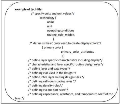
Fig 3: Technology File Example.
In VLSI physical design, tech files establish the bridge between design and manufacturing teams. These files communicate design intent and constraints, enabling foundries to precisely replicate the chip layout on silicon wafers. Any deviation from these documented specifications could result in design failures, yield losses, or compromised chip performance.
4. Design Constraints:
Design constraints encompass a range of specifications that guide the physical design process. These constraints include timing requirements, specifying critical parameters such as clock frequencies and maximum allowable delays. Power constraints outline limits on power consumption, a critical factor in modern IC design due to the increasing emphasis on energy efficiency. Additionally, area constraints dictate the maximum dimensions or chip size, ensuring that the final layout fits within the intended form factor. These constraints collectively serve as a compass, guiding the design towards meeting its performance, power, and size targets.
The SDC constraints or timing constraints contain the following information of design requirements:
- Create a clock definition.
- Generated clock definition.
- Virtual clock.
- Input delay.
- Output delay.
- Max delay.
- Min delay.
- Max transition.
- Max capacitance.
- Max fanout.
- Clock latency.
- Clock uncertainty.
Clock exceptions are also present in SDC. like.,
- Multicycle paths.
- False paths.
- Half cycle paths.
- Disable timing arcs.
- Case analysis.
These are timing constraints and used to meet the timing.
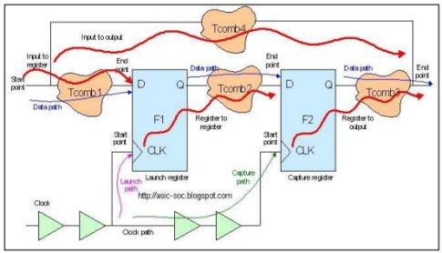
Fig 4: Timing Path Classification for Design.
SDC files define timing constraints such as setup and hold times, clock frequencies, and maximum path delays. These constraints ensure that the design operates correctly in terms of timing, preventing signal integrity issues and optimizing performance. The file specifies the characteristics of clocks used in the design, including their frequencies, sources, and relationships. This helps the tools accurately distribute and synchronize clocks across the design. SDC files include information about input and output ports, specifying input delay, output load, and other characteristics. This helps in optimizing power, signal quality, and overall design performance.
The constraints in SDC files are used for static timing analysis (STA) to validate that the design meets its timing requirements. They are critical in ensuring the design's correctness before fabrication. SDC files act as a common language between different teams working on the design, toolsets, and foundries. They ensure consistent design specifications and constraints throughout the development process. Design tools rely on the information in SDC files to make informed decisions during synthesis, place-and-route, and other implementation steps. This streamlines the design flow and reduces the likelihood of errors. As design iterations are performed, the SDC file helps in refining the design layout based on feedback from analysis tools. This iterative process leads to improved design quality.
An SDC constraint file in physical design is a critical document that provides a comprehensive set of instructions and limitations to guide the transformation of a logical design into a physically implementable layout. Its usage and importance revolve around achieving design goals, ensuring correctness, enabling collaboration, and optimizing the design for manufacturability and performance.
5. Floorplan:
In the context of integrated circuit (IC) design and architecture, a floorplan is a high-level representation that defines the placement and arrangement of various functional blocks, and components on a semiconductor chip. The floorplan is a critical step in the physical design stage of chip development and serves as the foundation for subsequent steps such as placement, clock tree synthesis, routing, and manufacturing. It essentially establishes the initial layout of the chip's elements and their relationships, helping to ensure that the design goals and constraints are met.
Key aspects of a floorplan include:
- Block Placement: This involves determining the approximate positions of different functional blocks or modules on the chip. Efficient block placement can lead to better overall performance, reduced power consumption, and improved thermal characteristics.
- Area Allocation: The floorplan allocates specific areas of the chip for different blocks or functional units, considering their size and importance. This helps to optimize the use of available space and ensures that critical blocks get adequate resources.
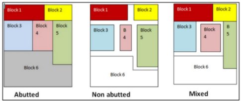
Fig 5: Different types of floorplan techniques.
- Power and Signal Distribution: The floorplan also outlines how power and ground distribution networks will be routed across the chip. It considers the need for uniform power delivery and signal integrity, minimizing delays and noise.
- Routing Channels: Floorplanning defines the locations and dimensions of routing channels, which are regions reserved for later stages of routing where interconnections between blocks will be established. Proper channel planning is crucial for ensuring efficient and congestion-free routing.
- IO (Input/Output) Placement: It determines where the input and output pins or pads will be located. These points provide the interface for external connections and must be strategically positioned for optimal performance and ease of testing.
- Clock Distribution: The floorplan also plays a role in planning the distribution of clock signals across the chip. Clocking strategies are critical for synchronizing different parts of the design and ensuring proper functioning.
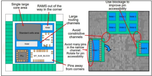
Fig 6: Some Guideline for Good Floorplan. [Image Source: Adam Teman]
In the floorplan, the size and shape of the chip or block are defined. Macro and IO cell placement is getting placed in such a way that effective routing space is available between the channel region and between the macro and IO regions. For standard cell placement, we keep the contiguous core area for standard cell placement and optimization strategy from the target cell library. In summary, a floorplan is a critical blueprint for the physical layout of an integrated circuit, guiding subsequent design steps and impacting performance, power efficiency, thermal characteristics, and manufacturability.
6. Power Distribution Network (PDN) Requirements:
The Power Distribution Network (PDN) plays a pivotal role in the realm of Very Large-Scale Integration (VLSI) physical design. It is an essential component of any integrated circuit (IC) that ensures a reliable and efficient supply of power to all the components within the chip. As VLSI technology has evolved, PDN design has become increasingly critical due to the escalating challenges posed by shrinking transistor sizes, higher clock frequencies, and increased power densities.
In VLSI integrated circuits, the power distribution network is responsible for delivering a stable and sufficient supply of power to all the functional blocks, gates, and transistors. It consists of a network of metal traces, vias, and power/ground planes that are strategically laid out across the chip. The primary purpose of the PDN is to ensure that every part of the chip receives the required voltage levels without excessive voltage drop, noise, or other powerrelated issues. The PDN includes two main types of nodes: power nodes and ground nodes. Power nodes carry the supply voltage, while ground nodes provide a reference point for the circuit's operation. These nodes are interconnected using metal layers and vias to form a complex network that spans the entire chip.
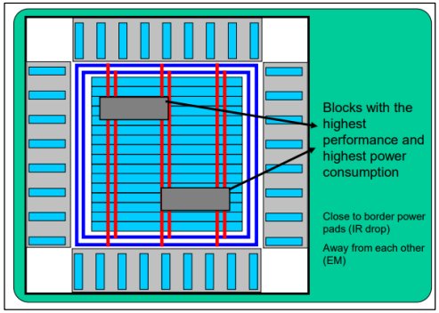
Fig 7: Power Plan Strategy. [Image Source: Adam Teman]
Importance of the Power Distribution Network (PDN) in VLSI Physical Design:
- Voltage Stability and Noise Mitigation: One of the central roles of the PDN is to maintain a consistent and stable supply voltage across the chip. Variations in voltage can lead to erroneous behavior of the circuitry, such as timing violations, reduced performance, and increased susceptibility to errors. The PDN must be designed to minimize voltage drop, which occurs due to the resistance of the metal traces and vias, and to suppress voltage noise caused by transient current fluctuations.
- Clock Distribution and Timing: The power network also plays a vital role in distributing the clock signal throughout the chip. Clock signals are sensitive to timing variations caused by voltage fluctuations. A well-designed PDN helps ensure that the clock signal arrives at all parts of the chip with minimal skew and delay, which is crucial for synchronous circuit operation and overall system performance.
- Heat Dissipation and Thermal Management: As transistor sizes continue to shrink, power densities increase, leading to higher heat generation within the chip. The PDN design must facilitate efficient heat dissipation by distributing power and ground connections strategically. Overheating can lead to performance degradation, reduced reliability, and even catastrophic failures.
- Signal Integrity: The PDN can also influence signal integrity, especially in highspeed designs. Voltage fluctuations in the power network can induce noise in the signals, leading to timing violations and data corruption. A well-designed PDN helps maintain a clean and noise-free environment for signal propagation.
Designing an efficient and robust PDN involves addressing several critical considerations and challenges:
- IR Drop: IR drop refers to the voltage drop across the metal traces and vias due to the resistance of the materials. This drop can lead to variations in supply voltage, affecting circuit performance. Minimizing IR drop requires careful placement of power and ground connections, as well as optimizing the width and spacing of metal traces.
- Decoupling Capacitors: Decoupling capacitors are strategically placed to provide local charge storage and reduce voltage fluctuations caused by sudden changes in current demand. Their placement and sizing impact the overall PDN performance.
- Power Gating and Dynamic Voltage Scaling: Power gating involves turning off power to specific blocks when they are not in use, reducing power consumption. Dynamic voltage scaling adjusts the supply voltage based on the workload. Both techniques affect PDN design by introducing additional power domains and voltage islands.
- Package-Board Interaction: The interaction between the chip's PDN and the package's power distribution can lead to impedance mismatches and resonances that degrade power delivery. Co-design between chip and package is crucial to mitigate such issues.
- Electromigration: High current densities in metal traces can lead to electromigration, where material is displaced due to the movement of electrons. This issue is crucial to address at below metal layers in physical design. By designing robust PDN structure we can avoid creation of hillocks and void in metal layers. Due to this reliability issue we may face functional failure over a time with an intended design.
- Thermal Management: Efficient heat dissipation is essential to prevent thermalinduced failures. The PDN layout must accommodate thermal vias and consider the thermal paths from power-generating blocks to the heatsink.
- Hierarchical Design: Modern designs are often hierarchical, with multiple levels of power domains. Ensuring consistent power delivery across these levels requires careful planning and analysis.
The Power Distribution Network (PDN) is a critical component of VLSI physical design that ensures reliable and efficient power delivery to integrated circuits. Its importance has grown with the increasing complexity, shrinking sizes, and higher power densities of modern ICs. A well-designed PDN minimizes voltage drop, noise, and other power-related issues, leading to improved performance, reliability, and manufacturability of the chips. Addressing challenges such as IR drop, decoupling, power gating, and thermal management requires a comprehensive understanding of PDN design principles. As technology continues to advance, PDN design remains a crucial enabler for achieving high-performance, low-power, and reliable integrated circuits.
7. Clock Tree Specifications:
In designs involving clock signals, the clock tree specification is essential. Clock signals synchronize the operations of different components within the circuit, and an effective clock tree is imperative for ensuring balanced and low-skew clock signals. The clock tree specification provides details on the placement and routing of clock distribution components, optimizing clock signal propagation and synchronization across the entire design.
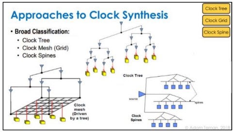
Fig 8: Clock Tree Classification. [Image Source: Adam Teman]
The importance included the capability of CTS to make the design time clean and bring the clock tree variations down by reducing the buffer count in the design. Various challenges were addressed in the tree building stage and the experiments performed yielding results. Clock tree building involves intense effect on the timing and power of the design and hence the clock tree needs to be built with intense care.
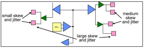
Fig 9: Balancing Clock Skew – A CTS Target. [Image Source: Adam Teman]
In the context of digital integrated circuit design, the clock tree is a crucial component of the physical design process. It involves the distribution of clock signals across a chip to ensure synchronous operation of all the sequential elements (like flip-flops) in the design. The clock tree specification refers to the set of guidelines and constraints that determine how the clock distribution network is designed and implemented.
The clock tree specification is important for several reasons:
- Timing and Synchronization: In digital circuits, all flip-flops and sequential elements need to be triggered by the same clock signal to ensure proper synchronization. A well-designed clock tree helps maintain consistent timing across the chip, preventing issues like clock skew (variations in arrival times of clock signals) that can lead to data corruption and reduced circuit performance.
- Minimizing Clock Skew: Clock skew, which is the variation in arrival times of clock signals at different parts of the chip, can cause timing violations and reduce circuit performance. The clock tree specification defines design rules and techniques to minimize clock skew, ensuring that clock signals arrive at different parts of the chip as uniformly as possible.
- Power Distribution: Clock distribution consumes a significant portion of the power budget in digital circuits. The clock tree specification can include guidelines to minimize power consumption while maintaining signal quality. Techniques like clock gating and voltage scaling can be used to reduce power consumption in the clock distribution network.
- Signal Integrity: Clock signals are high-frequency signals that can be susceptible to noise and interference. The clock tree specification may include guidelines for designing a low-impedance clock distribution network to minimize signal degradation and ensure proper clock signal integrity.
- • Layout and Routability: The clock tree specification influences the placement and routing of clock distribution wires across the chip. Well-designed clock trees consider the layout and routing constraints of the fabrication process, ensuring that the clock signals can be efficiently routed without causing congestion or violating design rules.
The clock tree specification plays a critical role in ensuring that the clock distribution network is designed to meet timing, power, signal integrity, and manufacturability requirements. A well-designed clock tree is essential for the overall performance, reliability, and yield of integrated circuits.
8. Physical/Layout Design Rules:
In the context of integrated circuit (IC) design, physical design rules refer to the specific guidelines and constraints that dictate how the layout of various components and structures on a semiconductor chip should be created. These rules ensure that the final manufactured chip functions correctly and reliably. Physical design rules are critical because they govern how different elements like transistors, interconnects, and other components are positioned and interconnected on the chip's surface.
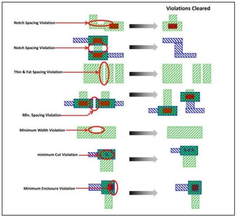
Fig10: Layout Design Rule Illustration.
Here are some common physical design rules:
- Design Rule Checks (DRCs): These are automated checks performed by design tools to ensure that the layout adheres to the specified physical design rules.
- Minimum and Maximum Metal/Interconnect Width and Spacing: These rules define the minimum and maximum allowable widths and spacings for metal interconnects that connect different parts of the circuit. These rules ensure that signals can be routed without causing shorts or signal integrity issues.
- Contact and Via Rules: These rules define the size and placement of contacts and vias used to connect metal layers, ensuring proper electrical connections between different layers.
- Well and Substrate Contact Rules: Guidelines for the placement and size of contacts that connect to different wells or substrate regions, important for creating distinct regions with different electrical characteristics.
- Poly to Active (Poly-to-Active) Spacing: This rule governs the distance between the polysilicon gate material and the active area of the transistor to prevent leakage or unintended interactions.
- Metal Density Rules: These rules limit how closely metal lines can be placed to avoid excessive heat generation or electromigration issues.
- Well-Tap Rules: Guidelines for adding well-tap structures that provide additional connections to substrate or well regions for better grounding and noise immunity. iii. Antenna Rules: These rules prevent the buildup of charge during the manufacturing process by requiring proper connections to ground or power.
- Electromigration and IR Drop Rules: These rules deal with the potential for excessive current density causing material degradation (electromigration) and voltage drop (IR drop) across interconnects.
It's important to note that physical design rules can vary based on the specific manufacturing process, technology node, and design requirements. Designers need to adhere to these rules meticulously to ensure the functionality, reliability, and manufacturability of the final chip. Non-compliance with physical design rules can lead to performance issues, manufacturing defects, or even complete chip failure.
9. Design for Manufacturing (DFM) Guidelines:
Design for Manufacturing (DFM) guidelines focus on optimizing the layout for manufacturability. These guidelines take into consideration the intricacies of various fabrication processes, such as lithography, etching, and material depositions. By aligning the layout with DFM principles, designers enhance the likelihood of achieving a high yield during fabrication, minimizing defects, and ensuring consistent performance across fabricated chips.
During route, apply additional design for manufacturing (DFM) and/or design for yield (DFY) rules:
- Via reduction
- Redundant via insertion
- Wire straightening
- Wire spreading
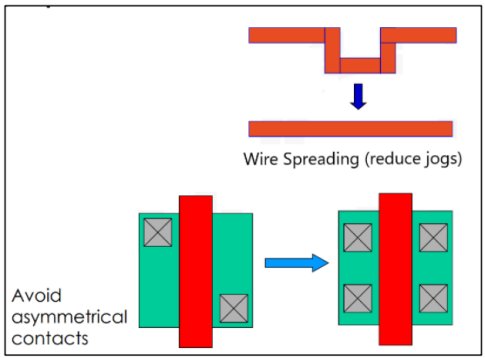
Fig 11 : DFM rule to increase yield.
Post-route via optimization includes incremental routing for the minimization of vias and replacement of single vias with multi-cut vias.
These operations are required for:
- Reliability: The ability to create reliable vias decreases with each process node. If a single via fails, it creates an open and the circuit is useless.
- Electromigration: Electromigration hazards are even more significant in vias, which are essentially long, narrow conductors.

Fig 12: Via Optimization.
Wire spreading is also the part of DFM techniques to lower capacitance and better signal integrity plus to lower susceptibility to shorts or opens due to random particle defects.
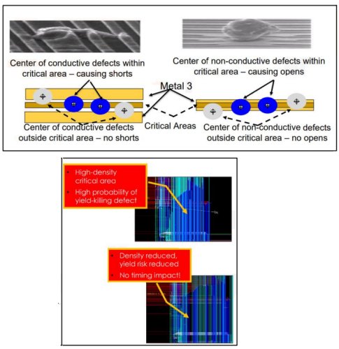
Fig13: Wire Spreading to Avoid Shorts and Open
Incorporating Design for Manufacturing (DFM) principles during the physical design stage of product development can result in significant benefits, including cost savings, improved quality, faster time to market, and enhanced collaboration between design and manufacturing teams. It's a strategic approach that aims to create products that are not only innovative and functional but also practical to manufacture and assemble.
10. Testability Requirements:
The testability of a design is a crucial consideration for quality assurance and fault detection. Testability requirements provide instructions for incorporating features such as scan chains, built-in self-test (BIST) structures, and other techniques that enable effective testing of the fabricated chips. These features facilitate the detection of defects and the assessment of chip functionality, enhancing the overall reliability of the product.
Testability is critical for the following reasons:
- Defect Detection: Testability techniques allow for the detection of manufacturing defects, such as open and short circuits, before the product reaches the final production stage.
- Early Bug Identification: By identifying and addressing design bugs early, the cost and effort of fixing issues later in the production cycle are minimized.
- Quality Assurance: Rigorous testing during the physical design phase ensures that the final product meets quality and reliability standards.
- Cost and Time Savings: Early defect detection and bug fixing reduce costly rework and production delays, leading to cost and time savings.
- Optimization and Iteration: Testability enables iterative design optimization based on testing feedback, resulting in an improved final product.
Design for Testability (DFT):
DFT involves designing hardware components or systems in a way that makes them easier to test. This can include features that enhance testability and diagnostic capabilities. An example of DFT is the insertion of scan chains for easy access to internal registers. Scan chains allow external testers to manipulate and observe internal states of a chip, aiding in functional testing and debugging.
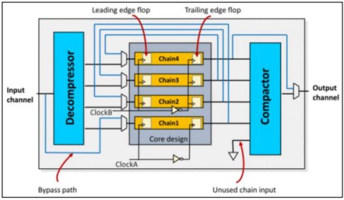
Fig14 : Compression with Scan Chains that Start with Leading Edge Flops and Ending in Trailing Edge Flops. [Source: blogs.sw.siemens.com]
Built-In Self-Test (BIST) Logic:
BIST is a technique where testing capabilities are integrated directly into the hardware design. BIST logic generates test patterns, applies them to the circuit, and analyzes the responses to detect faults. An example of BIST logic is a memory controller with built-in test patterns and error detection mechanisms. This controller can autonomously test memory cells and identify faulty ones without requiring external test equipment.
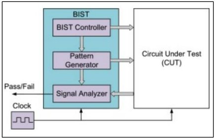
Fig15 : Built-in self-test architecture.
Testability in the physical design stage is essential for defect detection, bug identification, quality assurance, cost and time savings, and design optimization. DFT techniques like scan chains enhance testability by providing easy access to internal components, while BIST logic integrates testing capabilities directly into the design, improving the efficiency and effectiveness of testing processes. By incorporating these techniques, engineers can ensure the reliability and performance of hardware products while minimizing production costs and time-to-market.
11. Hierarchy and Partitioning Strategy:
The field of Very Large-Scale Integration (VLSI) involves designing and fabricating complex integrated circuits (ICs) that contain millions to billions of transistors on a single chip. The physical design of these ICs involves laying out the circuit components, interconnections, and other structures to achieve optimal performance, power consumption, and area utilization. Two critical aspects of VLSI physical design are hierarchy and partitioning strategy, which play pivotal roles in managing the complexity of modern chip designs. In this article, we will delve into these concepts, their significance, and how they are employed in the physical design process.
Hierarchy in VLSI Physical Design:
Hierarchy is a fundamental principle in VLSI physical design that aims to manage the complexity of large circuits by breaking them down into smaller, more manageable modules or blocks. Each module represents a functional unit of the design, which can range from individual gates to larger sub-circuits. Hierarchy enables engineers to tackle the design process in a systematic manner, starting from high-level abstractions and gradually refining the design at lower levels of detail.
Significance of Hierarchy:
- Abstraction and Modularity: Hierarchy allows designers to work at different levels of abstraction. At the top level, the entire chip is represented, while at lower levels, different modules are represented with increasing detail. This modularity facilitates easier design, debugging, and verification.
- Design Reusability: By breaking down a complex design into reusable modules, engineers can save time and effort by reusing proven blocks in different projects. This can lead to quicker design iterations and shorter time-to-market.
- Efficient Collaboration: Hierarchy promotes collaboration among different design teams or engineers working on different parts of the chip. Each team can focus on their respective modules without having to understand the entire design in detail.
- Easier Debugging: Debugging a large monolithic design can be extremely challenging. Hierarchy allows designers to isolate and debug issues within specific modules, reducing the complexity of the debugging process.
- Performance Optimization: By concentrating on specific modules, designers can apply optimizations tailored to the requirements of each module. This can lead to better performance, power consumption, and area utilization.
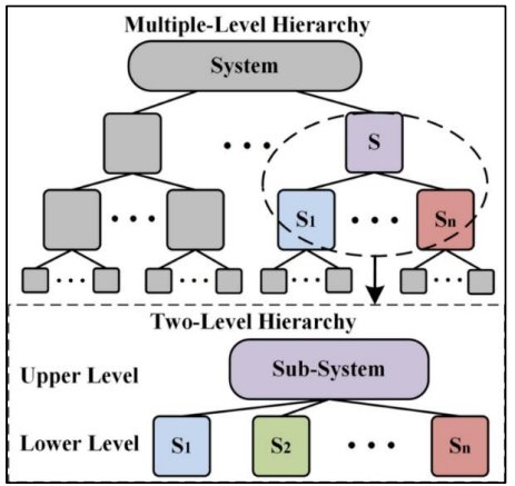
Fig 16: Multiple level Hierarchy and Partition of System/Chip
Hierarchy in VLSI physical design is typically organized into several levels, including.
- System Level: This is the highest level of hierarchy, where the overall chip architecture is defined. It includes major components, their interconnections, and high-level considerations such as power distribution and clocking.
- Block Level: At this level, the chip is divided into functional blocks or modules. These blocks might represent different subsystems or major components of the design.
- Sub-block Level: Each block is further divided into sub-blocks, which could be specific functional units or smaller sub-circuits.
- Leaf Cell Level: The lowest level of hierarchy contains individual cells, such as standard cells, flip-flops, and other basic building blocks. These cells are the smallest components used to create the design.
Partitioning Strategy in VLSI Physical Design:
Partitioning is a crucial strategy in VLSI physical design that involves dividing a chip into smaller, more manageable regions or partitions. Each partition can then be designed and optimized separately, and later integrated to form the complete chip layout.
Partitioning can occur at various levels of hierarchy, and the choice of partitioning strategy has a significant impact on the overall design quality.
Significance of Partitioning Strategy:
- Complexity Management: Modern chips are immensely complex, and partitioning allows designers to handle this complexity by breaking it down into smaller pieces that can be managed more effectively.
- Parallelism and Resource Utilization: By partitioning a design, multiple teams or tools can work on different partitions simultaneously. This parallel approach speeds up the design process and utilizes available computational resources more efficiently.
- Optimization Flexibility: Different partitions of a chip may have distinct requirements or constraints. Partitioning enables designers to optimize each region based on its specific needs, such as power consumption, performance, or area utilization.
- Reduced Interconnect Lengths: Carefully planned partitioning can lead to shorter interconnect lengths between different functional blocks, resulting in reduced signal delays and improved overall performance.
Partitioning Strategies are as below.
- Top-Down Partitioning: In this approach, the chip is divided into large functional blocks based on the system-level architecture. These blocks are then further partitioned into smaller modules. Top-down partitioning is effective for managing high-level design considerations but might result in less optimal partition sizes at lower levels.
- Bottom-Up Partitioning: This approach starts with small modules or cells and groups them into larger blocks. The aggregation process continues until the entire chip is partitioned. Bottom-up partitioning is useful for achieving balanced partition sizes, but it might not consider higher-level design goals effectively.
- Hierarchical Partitioning: This strategy combines both top-down and bottom-up approaches. It involves partitioning the design at multiple hierarchy levels, starting from the system level, and refining the partitions as the design progresses to lower levels. This approach aims to balance system-level goals with local optimizations.
- Clustering-Based Partitioning: Clustering algorithms analyze the design's connectivity and attempt to group closely related components into the same partition. This can help reduce interconnect lengths and enhance performance.
- Constraint-Driven Partitioning: This approach considers specific design constraints, such as signal integrity, power distribution, or timing requirements, when creating partitions. It ensures that each partition meets these constraints while optimizing for other objectives.
Hierarchy and partitioning strategy are critical concepts in VLSI physical design that enable engineers to manage the complexity of modern chip designs effectively. Hierarchy provides a structured approach to design by breaking down the circuit into manageable modules, facilitating collaboration, design reuse, and optimization. Partitioning strategy, on the other hand, divides the chip into smaller partitions to manage design complexity, utilize resources efficiently, and achieve performance goals. Both concepts play essential roles in ensuring the success of VLSI designs, from initial architecture definition to the final layout implementation. As chip designs continue to evolve and become more intricate, the principles of hierarchy and partitioning will remain foundational in achieving efficient and effective VLSI physical designs.
12. IP Blocks and Macros:
In the context of physical design in the field of semiconductor and integrated circuit (IC) design, IP blocks and macros refer to pre-designed and pre-verified functional components that can be integrated into a larger chip design. These components are essentially building blocks that serve specific functions, such as memory, arithmetic units, interfaces, clock generation, and more. Integrated circuits often incorporate intellectual property (IP) blocks or macros obtained from third-party sources. These pre-designed components serve as functional building blocks that can be integrated into the overall design. The physical design process requires information about these IP blocks, including their dimensions, pinouts, and usage guidelines. Integrating IP blocks effectively accelerates the design process and leverages existing solutions to meet design requirements.
- Intellectual Property (IP) Blocks: Intellectual Property blocks are pre-designed and pre-verified functional units that can be integrated into larger designs. They can range from simple components like basic logic gates and flip-flops to complex units such as microprocessors, memory controllers, and communication interfaces. These blocks are designed to be reusable, enabling designers to incorporate proven, standardized functionality without having to recreate it from scratch.
- • Macros: Macros are a specific type of IP block that encompasses larger functional units. Unlike general-purpose IP blocks, macros typically have well-defined functionalities, like memory cells, standard cells (basic logic gates), and analog components. They are designed to be parameterizable, allowing them to be customized for specific design requirements. Macros can be further classified as soft macros and hard macros:
- Soft Macros: These are synthesized designs that are parameterizable and can be customized to fit varying design specifications. Soft macros provide a balance between flexibility and efficiency, as they can be optimized for different technologies and design constraints.
- Hard Macros: Hard macros are fixed, layout-level representations of a functional block. They are optimized for specific technology and performance criteria. Hard macros often offer better performance and power efficiency compared to soft macros, but they lack the customization options that soft macros provide.
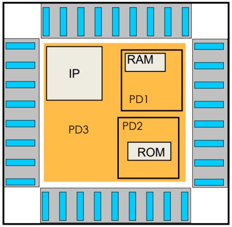
Fig17: IP and Macro Placement at Core Area in a Block Level Design.
Significance of IP Blocks and Macros in VLSI Physical Design:
- Design Reusability: One of the most significant advantages of IP blocks and macros is their reusability. Designers can leverage existing, well-tested IP blocks instead of reinventing the wheel for every project. This reduces design time, minimizes potential errors, and accelerates the overall design process.
- Time-to-Market: The integration of IP blocks and macros accelerates the design process, leading to shorter time-to-market for new products. Designers can focus on the unique aspects of their projects while relying on trusted IP components for the common functionalities. This agility is crucial in competitive industries where faster product releases can yield a significant market advantage.
- Focus on Innovation: By utilizing pre-designed IP blocks, designers can allocate more time and resources to the innovative aspects of their designs. Instead of spending time on routine or standardized components, they can concentrate on pushing the boundaries of performance, power efficiency, and functionality.
- Quality and Reliability: IP blocks and macros undergo rigorous testing and verification processes before being made available. Integrating these proven components into a design enhances its quality and reliability. This is especially critical for safety-critical applications like medical devices and automotive electronics.
- Optimization and Performance: Macros, especially hard macros, can be optimized at the physical layout level to achieve superior performance and power efficiency. This optimization takes advantage of the specific characteristics of the target technology and manufacturing process.
- Reduced Design Complexity: Modern IC designs are incredibly complex, and managing every aspect of a design from scratch can be overwhelming. IP blocks and macros simplify the design process by breaking it down into manageable units, reducing the overall complexity and improving design comprehension.
- Industry Standards and Ecosystem: The availability of standardized IP blocks fosters an ecosystem where designers, manufacturers, and tool providers collaborate. This ecosystem promotes interoperability and compatibility, making it easier for designers to integrate different components seamlessly.
- • Risk Mitigation: Using well-tested IP blocks mitigates the risk of design errors and failures. These blocks have already been subjected to extensive testing, reducing the likelihood of critical errors that might lead to project delays or costly recalls.
Implementation Challenges and Considerations:
- IP Quality and Compatibility: Choosing high-quality IP blocks that are compatible with the target technology and design constraints is essential. Poorly designed or incompatible IP can lead to integration issues and suboptimal performance.
- Legal and Licensing Issues: When using third-party IP, designers must ensure that they adhere to licensing agreements and intellectual property rights. Violations can lead to legal complications and disruptions in the design process.
- Customization and Integration: While IP blocks offer reusability, customization may still be necessary to meet specific project requirements. Designers must strike a balance between customization and integration effort to achieve the desired outcome efficiently.
- Verification and Testing: Although IP blocks undergo thorough testing, integration can introduce new issues that need to be verified. Ensuring the proper functionality and performance of integrated IP is crucial to avoid post-manufacturing failures.
- Security Concerns: Integrating third-party IP can introduce security vulnerabilities if not adequately vetted. Designers must consider potential security risks and implement measures to protect sensitive information and proprietary designs.
In the intricate realm of VLSI physical design, IP blocks and macros stand as indispensable tools that streamline the creation of complex integrated circuits. Their significance lies in their ability to enhance design reusability, reduce time-to-market, foster innovation, and improve overall design quality. While challenges related to compatibility, customization, and legal considerations exist, the benefits of leveraging IP blocks and macros outweigh the drawbacks. As technology continues to advance, the role of IP blocks and macros will remain pivotal in shaping the future of VLSI design, enabling designers to push the boundaries of what's possible in the realm of semiconductor technology.
13. LEF and DEF Formats:
In the context of VLSI physical design, two essential formats are used to describe the physical layout and characteristics of the integrated circuit: Library Exchange Format (LEF) and Design Exchange Format (DEF). These formats play a critical role in facilitating the exchange of design data between different tools and stages of the physical design flow, aiding in collaboration, optimization, and manufacturability.
Library Exchange Format (LEF):
The Library Exchange Format (LEF) is a standard format used to describe the characteristics of standard cells, macros, and other components that are part of a semiconductor library. A library, in this context, consists of a collection of predefined circuit elements that designers use to assemble and create their integrated circuit designs. These elements include gates, flipflops, multiplexers, and other building blocks. LEF files contain essential information about these elements, such as their physical dimensions, pin placements, routing information, and other relevant properties. Some of the key components of an LEF file include:
- Cell Definitions: LEF files define the geometric shapes, layers, and other parameters that define the physical appearance of each cell or macro.
- Pin Placements: The positions of input, output, and power pins for each cell are specified in the LEF file. This information is crucial for the placement and routing stages of physical design.
- Layer Information: The LEF format includes details about the metal layers, diffusion layers, and other layers used in the fabrication process. This information helps in correctly placing and routing the components.
- Spacing and Density Rules: LEF files can also specify design rules related to spacing, density, and other layout-related constraints. These rules ensure that the final layout adheres to the manufacturing process requirements.
- Routing Information: LEF files may provide guidelines for routing connections to and from the cell, helping ensure proper signal integrity.
Design Exchange Format (DEF):
The Design Exchange Format (DEF), on the other hand, focuses on describing the top-level design, which includes the placement of cells, routing of interconnections, and other designrelated data. The DEF file acts as a bridge between different stages of the physical design flow, enabling communication between tools responsible for placement, routing, and verification.
The DEF format captures several critical aspects of the design:
- Cell Placement: DEF files provide information about the placement of cells or components on the chip's layout canvas. Proper placement significantly impacts the circuit's performance, power consumption, and manufacturability.
- Netlist and Interconnections: The connectivity between cells and their interconnections is defined in the DEF file. This information guides the routing stage to create a physical wiring layout that connects the various components.
- Physical Constraints: DEF files can include constraints related to spacing, alignment, and other physical design rules. These constraints help ensure that the final layout meets manufacturing and performance requirements.
- Power and Ground Distribution: Power and ground networks are crucial for the functionality and reliability of the design. DEF files may provide guidelines for the distribution of power and ground connections.
- Timing Constraints: Timing information, including constraints on signal propagation delay, setup and hold times, is often included in the DEF file to guide the optimization of the design for performance.
LEF and DEF Integration in the Design Flow:
The LEF and DEF formats are intimately connected and play a crucial role in the VLSI physical design flow. The following steps highlight how these formats are integrated:
- Library Characterization: Semiconductor manufacturers provide libraries of standard cells and macros that are characterized and described using the LEF format. These libraries serve as the foundation for building complex designs.
- Cell Placement: The placement tool uses the information from LEF files to position the cells on the chip's layout canvas. Proper placement aims to optimize for factors like performance, power consumption, and thermal considerations.
- Routing: The routing tool leverages the DEF file to route the interconnections between cells. The information about cell locations and pin connections is vital for generating efficient and manufacturable routing solutions.
- Design Closure: The iterative nature of physical design often requires several iterations to meet design goals. LEF and DEF files are refined and updated as the design progresses, ensuring that the layout conforms to the desired specifications.
Benefits and Challenges:
The LEF and DEF formats provide several benefits to the VLSI physical design process:
- Interoperability: The formats enable different tools from various vendors to work seamlessly together. Design teams can choose the best tools for each stage while maintaining data integrity.
- Efficiency: The formats encapsulate critical information about components, placement, routing, and constraints, reducing the need for manual intervention and reducing the risk of errors.
- Collaboration: Design teams often span different geographical locations. The LEF and DEF formats facilitate collaboration by providing a standardized way to share design data.
- Optimization: With accurate and detailed information from LEF and DEF files, designers can make informed decisions to optimize performance, power consumption, and manufacturability.
However, there are challenges associated with these formats:
- Complexity: Creating and maintaining LEF and DEF files can be complex and timeconsuming, particularly for large and intricate designs.
- Version Compatibility: As tools and standards evolve, compatibility issues can arise when using different versions of LEF and DEF formats.
- Accuracy: Inaccurate or incomplete data in LEF or DEF files can lead to design errors, poor performance, and manufacturability issues.
- Data Volume: The amount of data in large designs can be substantial, leading to potential performance and storage challenges when working with LEF and DEF files.
In the realm of VLSI physical design, the Library Exchange Format (LEF) and Design Exchange Format (DEF) are instrumental in enabling the translation of logical designs into physically manufacturable layouts. LEF files provide detailed descriptions of standard cells and macros, while DEF files capture the placement, routing, and constraints of the overall design. These formats facilitate interoperability, collaboration, and optimization throughout the physical design flow, allowing designers to create efficient and reliable integrated circuits. While there are challenges associated with their creation and management, LEF and DEF formats remain indispensable tools in the development of advanced semiconductor devices.
Conclusion:
The VLSI physical design stage is a pivotal juncture in the journey from a logical design to a manufacturable and functional semiconductor chip. The prerequisites for this stage, encompassing logical design, technology library, floorplan, power distribution network requirements, clock tree synthesis constraints, design rules, manufacturing process information, and timing constraints, form the bedrock upon which successful physical design is built.
The significance of these prerequisites is profound. They empower an efficient design process, maintain functional correctness, enhance manufacturability, optimize performance, ensure predictable yield, and foster cost efficiency. A comprehensive understanding of these prerequisites equips design teams with the knowledge and foresight needed to navigate the complexities of VLSI physical design successfully.
In a field where miniaturization and performance are paramount, the adherence to prerequisites and the careful consideration of their importance stand as cornerstones of excellence in VLSI physical design. By aligning the design process with these prerequisites, engineers and designers pave the way for the creation of cutting-edge semiconductor chips that power the digital world.
Reference:
- IC Compiler™ II Design Planning User Guide, Version L-2016.03-SP4, September 2016
- IC Compiler Implementation User Guide, Version C-2009.06, June 2009
- Digital VLSI Design by Dr. Adam Teman
- Physical Design Essentials: An ASIC Design Implementation Perspective by Khosrow Golshan Conexant Systems, Inc. Newport Beach, CA
- https://solvnet.synopsys.com/
- https://blogs.sw.siemens.com/
About the Author:
Dhaval Shukla

Dhaval Shukla is working as an ASIC Physical Design Engineer at eInfochips (An Arrow Company). He has more than 5.5 years of experience in ASIC Physical Design. He has experience in the bock level implementation at lower technology nodes (3nm, 4nm, 22nm and 40nm) for ASIC chips, where his accountabilities include the Block level PnR, ECO Implementation and Complete Sign-off Closure. He has handled multiple complex blocks in terms of memories, power blocks and instance count in the design. His project exposure also includes the flow implementation like merge, Fill and PV (i.e., Antenna, DRC and LVS). He holds M.Tech degree in VLSI Design from Nirma Institute of Science & Technology, Ahmedabad.
Related Semiconductor IP
- NPU IP Core for Mobile
- NPU IP Core for Edge
- Specialized Video Processing NPU IP
- HYPERBUS™ Memory Controller
- AV1 Video Encoder IP
Related White Papers
- The role of cache in AI processor design
- The Growing Imperative Of Hardware Security Assurance In IP And SoC Design
- Bigger Chips, More IPs, and Mounting Challenges in Addressing the Growing Complexity of SoC Design
- VLSI Physical Design Methodology for ASIC Development with a Flavor of IP Hardening
Latest White Papers
- Transition Fixes in 3nm Multi-Voltage SoC Design
- CXL Topology-Aware and Expander-Driven Prefetching: Unlocking SSD Performance
- Breaking the Memory Bandwidth Boundary. GDDR7 IP Design Challenges & Solutions
- Automating NoC Design to Tackle Rising SoC Complexity
- Memory Prefetching Evaluation of Scientific Applications on a Modern HPC Arm-Based Processor