A 66-mW 3.4Gbps Transmitter PHY for HDMI Applications in 2.5V 40-nm CMOS
Cuneyt Demirdag 1, Chris Dietrich 1, Marcin Kowalewski 2,
Nelson Lam1, Dino Toffolon1, Zhinian Shu1
Synopsys®
Mississauga, Canada1
Gdansk, Poland2
Abstract :
This paper presents a low-power Synopsys® DesignWare® High Definition Multimedia Interface Transmitter (HDMI TX) PHY in a 2.5V 40-nm CMOS process. It employs a number of features for IP portability and ultra-low power consumption. The DesignWare HDMI TX IP includes a half-rate serializer, a low-power PLL and clocking scheme in addition to a novel TX architecture. The architecture is portable into both 2.5V and 1.8V process nodes, and makes use of a “supply-less” termination scheme that eliminates the need for a 3.3V supply. The Synopsys DesignWare HDMI TX PHY passes all electrical HDMI compliance specifications, achieves a power consumption of 49mW at 1.485Gbps (1080p-8 bit) and obtains a maximum operating frequency of 3.4Gbps.
I. Introduction
HDMI is rapidly becoming the global standard for connecting high-definition consumer products and PC interfaces. The HDMI standard outlines a 10.2Gb/s unidirectional interface for the transmission of high-definition multimedia content between HDMI sources (transmitters) and sinks (receivers). The interface consists of three 3.4Gb/s Transition Minimized Differential Signaling (TMDS) lanes as well as one TMDS Clock lane. These lanes carry audio/video data from the HDMI source to the HDMI sink.
In this paper, we present the Synopsys DesignWare HDMI TX PHY IP solution designed in a 40-nm low-power CMOS that displays best-in-class jitter, power consumption and area metrics. The DesignWare HDMI TX PHY is compliant to the HDMI v1.4 specification, including support for up to 16-bit Deep Color modes.
A top-level view of the presented DesignWare HDMI TX PHY, highlighting the main interface and connectivity between blocks, can be seen in Fig 1.
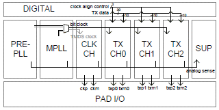
Fig 1 Top-level view of the DesignWare HDMI TX PHY
The clock generation and timing solution, encompassing the Prescale PLL (Pre-PLL) and Multiplying PLL (MPLL) blocks in Fig 1, will be presented in Section II. Since the HDMI specification indicates that HDMI allows many video format timings to be transmitted and displayed [3], this demands a timing solution that is extremely flexible as video input clocks ranging from 25MHz to 340 MHz must be supported.
The three TMDS lanes, indicated by the TX CH0, TX CH1, and TX CH2 blocks in Fig 1, are composed of 10-to-1 serializers followed by 5V tolerant TMDS drivers. These two-lane sub-blocks, along with ESD circuitry that meets the HDMI standard’s back-powering requirement, are discussed in Sections III, IV and V respectively.
All of the biasing for the DesignWare HDMI TX PHY is contained within the Support block (labeled SUP in Figure 1). This block is also responsible for performing the on-chip source termination resistance tuning for the PHY and will be presented along with built-in test features in Section VI.
Finally, laboratory measurements for the 40-nm DesignWare HDMI TX PHY IP testchip will be presented in Section VII.
II. Clock Generation and Distribution
The HDMI TX PHY uses two PLLs for clock generation and distribution: the Pre-PLL and the MPLL. The Pre-PLL is used to support deep color modes needed for pixel repetition and for input reference clock conditioning. The MPLL provides the transmitter with the high-speed clock in the range of 125MHz-1700MHz.
To support the various deep color modes, the Pre- PLL needs to generate an output clock that is 1X, 1.25X, 1.5X or 2X the reference pixel clock rate. These ratios correspond to color depths of 24-, 30-, 36- and 48-bits per pixel respectively. The Pre-PLL achieves these modes using two dividers: a programmable divider in its feedback path and a divider at the output of the Pre-PLL. For example, to achieve a ratio of 1.5X or 36-bits per pixel, the programmable divider ratio is set to divide by 6 and the output divider is set to divide by 4.
These two dividers are used further to implement pixel repetition modes that are required to support pixel rates less than 25MHz. For example, to support a pixel repetition mode of 3X, the programmable divider is set to divide by 6 and the output divider is set to 2.
The MPLL provides the transmitters with the highspeed serial rate clock. The jitter on this clock directly impacts the transmitted eye and, more importantly, it impacts the jitter of the recovered data at the receiver. Before we go into the detail of the MPLL architecture, we should understand how the data is recovered in an HDMI receiver.
The HDMI receiver receives both the data and the TMDS clock from the HDMI transmitter. The receiver uses the TMDS clock as a reference to a PLL with a 4MHz bandwidth to create a bit rate clock. This filtered bit rate clock is then used to clock in the TMDS data into the receiver’s clock domain for de-serialization, etc. Therefore, it is observed that the RX bit clock can have a different jitter profile than the TMDS data depending on how the TMDS clock reference to the RX is generated.
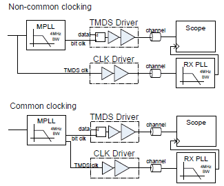
Fig 2 Non-common vs. common clocking jitter measurement
As can be seen in Figure 2, if the common clocking scheme is used, the generated RX bit clock will have been created from a TMDS clock whose jitter profile was already filtered by the MPLL. This will create an RX bit clock that has a different jitter profile than the data, as the reference TMDS clock would have been filtered twice - once by the MPLL and once by the ideal 4MHz PLL. This difference in jitter profiles will cause an increase in measured jitter in the RX.
In the non-common clocking scheme, the data arriving at the input to the receiver is clocked by the TX bit clock, which is the TMDS clock filtered by the MPLL. If the MPLL has the same bandwidth as the ideal 4MHz PLL, then when the RX creates its bit clock from the TMDS clock, the data will end up having a similar jitter profile as the RX bit clock. Therefore, the resultant jitter of the sampled data will be minimal, as none will be introduced by the difference between the jitter profiles of the TX and RX bit clocks. This was confirmed by simulation, and it can be concluded that the non-common clocking scheme offers the lowest jitter if the bandwidth of the TMDS PLL is kept close to the bandwidth of the receiver PLL at 4MHz. As a result, the MPLL is designed to use the noncommon clocking scheme with a constant bandwidth at around 4MHz despite a wide range of reference clock rates.
The MPLL uses a triple-loop self-biased PLL architecture [1, 2]. In this self-biased PLL, all the small signal parameters are related to the operating point of the VCO. Therefore, if the VCO frequency is kept within a small range, then (to a first order approximation) the bandwidth of the PLL can be kept relatively constant. If the VCO frequency is kept within a small range, then the feedback divider ratio (N) needs to change to accommodate the different reference clock rates (i.e., the pixel rate). This will have a large impact on the MPLL gain and, therefore, have a large impact on the bandwidth of the MPLL. To make the MPLL insensitive to the change in the divider ratio (N), the MPLL is designed to have a programmable scaling parameter that is equal to 1/N. Therefore, when N changes due to a change in pixel rate, the overall gain is unchanged. To the first order, the transfer function is unchanged and the constant bandwidth is achieved. However, since the VCO frequency still varies over a small range, as opposed to being fixed to a constant value, other scaling parameters need to be adjusted to keep the bandwidth close to 4MHz over all the video standards.
III. Serializer
There are three identical 10-to-1 serializers implemented in the DesignWare HDMI TX PHY - one for each data channel. The 10-to-1 serializer is implemented with a half-rate clocking scheme in order to reduce the operating frequency and power consumption of the PLL and associated clock buffers. However, a half-rate clock scheme requires using both clock edges to serialize the data. Therefore, an extra duty-cycle correction (DCC) circuit is needed inside the PLL to minimize TX jitter caused by duty-cycle error.
The serializer outputs two sets of differential signals: the “symbol” bit and the “trailer” bit. The “symbol” bit is the actual transmitted data, while the “trailer” bit is used for de-emphasis. The “trailer” bit is an inverted version of the “symbol” bit delayed by 1-bit time. The function of the “symbol” and “trailer” bits are further discussed in Section IV.
IV. TMDS Driver
There are four identical TMDS drivers implemented in the DesignWare HDMI [TX] PHY one for each of the three data channels and one for the clock channel. Fig 3 shows a block diagram of the TMDS driver. The key blocks in the TMDS driver includes the edge-rate control, the pre-driver, the output driver, the replica bias and the source termination.
The edge-rate control block is designed to slow down the output rise/fall time of the transmitter. A slow rise/fall time helps to reduce reflections especially when the source termination is removed. This block takes the serializer output and splits it into an early (fast) and a late (slow) path; the delay of the late path is longer than the early path. Consequently, the pre-driver and output driver also contain two paths one is driven by the early path+ and the other is driven by the late path.
The outputs of the edge-rate control block feed the pre-driver block. The pre-driver buffers these outputs and provides enough drive strength to drive the output driver. The pre-driver is implemented with core devices in the core supply domain, an implementation that consumes less power than conventional current mode logic (CML) in 3.3V or 2.5V supply domains.
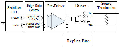
Fig 3 TX block diagram
The output current mode driver is composed of many finger cells that are driven by the “symbol” or “trailer” bits created from the serializer. As mentioned previously, there are also two paths for the early and late portions of the edge rate control.
A driver finger cell is shown in Fig 4. The core device, M1, is driven by the pre-driver outputs. It acts as a switch that enables the current mirror device, M2. A stress-free condition is guaranteed for M1 if the bias voltage, vb, is less than ‘(core supply+10%) - VgsM2’. The I/O device, MP, is driven by a bias voltage, vprot, generated from the 5V tolerant circuitry. In normal operation, vprot is equal to the I/O supply, and in powered off condition, vprot is a function of the pad voltage (e.g. vpad*0.5). This architecture [2] maximizes the use of core devices in the high-speed signal path, and consequently has lower power consumption than classical CML-based drivers.
The replica bias block defines the transmit output current and hence the transmit amplitude. The transmit amplitude is controlled by two input parameters the source termination setting and the amplitude setting. The source termination setting controls the source termination impedance in several coarse steps (e.g., open, 200W, 150W, 100W and 50W). The amplitude setting defines the singleended logic low level with respect to the supply. Also, the amplitude setting is dependent on the source termination setting. This dependency arises due to the need to compensate for the effect of different source termination impedances on the common mode voltage level. The transmit amplitude can be calculated with this equation:

where vref is a supply (vp25) referenced bandgap voltage, and R is the source termination resistance.
The replica bias is shown in Fig 4. It consists of a replica output driver, a replica far-end termination, a replica source termination and an opamp. The replica blocks are scaled to minimize power consumption.
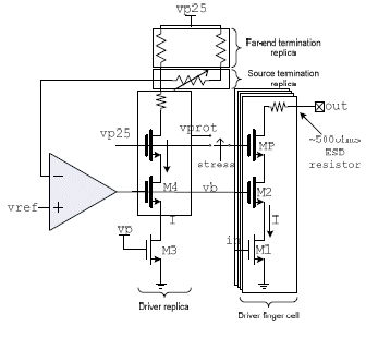
Fig 4 Replica bias and output driver fingers (note: source termination not shown)
There are several challenges involved in the design of the transmitter source termination. One of the main challenges is to implement the source termination with only a 2.5V power supply and 2.5V devices while the HDMI specification dictates the far-end termination voltage to be 3.3V±5%. Enforcing this design requirement allows the DesignWare HDMI TX IP to be implemented in processes where 3.3V I/Os are unavailable. However, it creates two problems: 1) enabling/disabling the source termination without a 3.3V supply; and 2) guaranteeing a device’s stressfree operation with/without the internal supply.
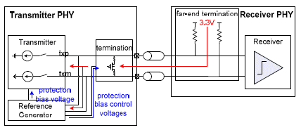
Fig 5 Source termination architecture.
The transmit source termination that was implemented into the HDMI testchip is shown in Fig 5. The tunable source termination is connected across the differential output with a pMOS switch and two poly resistors connected in a series. The switch can be enabled or disabled by a special levelshift- up (LSU) circuit. To disable the source termination, the logic high output voltage level from the LSU is applied to the pMOS switch. This LSU uses the transmitter’s common mode voltage (e.g., 3.05V) from the far-end termination as the logic high. Note: the common mode voltage level puts the resistor unit cell in a high impedance state such that it has a negligible effect on the overall impedance; however, the device is not completely shut off. A regulated bandgap voltage is used as the logic low level in the LSU circuit. Using this voltage level ensures that the pMOS source termination switches operate with no device stress (where Vgs and Vgd stress is less than 2.5V+10%).
The derived common mode reference voltage also generates a set of internal reference voltages that are used for stress protection. Because the internal reference voltages are derived from the far-end termination, device stress-free conditions are achieved in both normal operation and when the supply is absent. For example, the devices must be stress-free when an LCD TV (HDMI RX) is powered on and connected to a DVD player (HDMI TX) that is powered off.
Design for 5V tolerance is another criterion for the transmitter output stage. This requirement is based on the HDMI specification, as it mandates that no damage to the HDMI source or sink may result from the shorting of any combination of signals on the HDMI connector. This implies a possible 5V short scenario, as there is a 5V supply pin present. The proposed 5V protection circuit is shown in Fig 6.
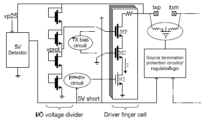
Fig 6 Simplified 5V protection circuit.
The 5V tolerant design covers the scenario where the HDMI TX supplies are grounded (or powered off). The 5V protection circuit is built using a 5V stress comparator, a voltage divider on the TMDS lines (which consumes current once voltage on the TMDS lines, txp or txm is > 4V), a regulator and a logic circuit that enables and disables portions of the output stage in source termination.
In a 5V stress condition the gate bias of the NMOS cascoded transistor, MP, is being switched from the I/O supply (e.g. 2.5V) to half the pad voltage to avoid any junction stress greater than the I/O supply (e.g. 2.5V + 10%). In order to protect the source termination, it is necessary to ensure that no current flows through the source termination in the case where txp=5V and txm=0V.
V. ESD
The primary ESD protection uses a Rail-Based ESD concept (Fig 7) where an ESD event is sensed by a 5V tolerant trigger circuit. Once an ESD event is detected, the trigger circuit activates the cascoded active mosfet clamps (TRIGA, TRIGB go high) in all I/O cells, thus the shock current is discharged through the common floating ESD rail. This approach significantly reduces I/O ring area and decreases I/O capacitance (which is crucial for high-speed designs).
Design criteria for this concept include preventing faulty triggering during normal operation, power-up sequences and latch-up tests. The design withstands ESD events up to 2kV based on the Human Body Model, 200V based on the Machine Model and 500V based on the Charged Device Model.
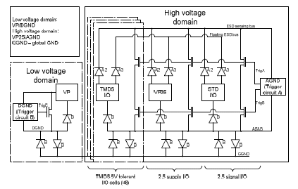
Fig 7 Primary ESD protection circuit
VI. Support and Test Blocks
The support block and built-in test and measurement circuitry complete the DesignWare HDMI TX IP design. The support block contains circuitry used for bias generation and source resistor calibration. An accurate bias voltage ladder is created with a band-gap generator to provide 32 levels to choose from for the TMDS data and clock transmit levels. The clock and data transmit levels can be set independently, such that the data channels can have higher or lower swing than the clock channel.
The resistor calibration block utilizes an off-chip 1.6kOhm 1% precision resistor to calibrate how many unit resistor cells should be switched on to generate exactly 50W of on-chip source resistance over process, voltage and temperature (PVT) variations.
There is extensive test and measurement circuitry built into the DesignWare HDMI TX PHY, including a 10-bit ADC and an undersampling scope. All of these test features are available via an I2C interface. The on-chip scope and ADC greatly reduce ATE cost and development time, and allow for accurate on-chip measurements without the need for expensive external equipment.
The on-chip sub-sampling scope was developed for capturing on-chip TX eye diagrams at all of the TMDS and clock output nodes. Separate scope blocks (a total of four) are put in all of the TX and clock channel outputs. The scope has two types of measurements: a fast 6-point pass/fail eye diagram and a full-resolution eye diagram with 512 time steps and 512 voltage steps. The TX data stimulus is automatically generated by a built-in self-test block that includes a PRBS generator. Voltage margining is performed by applying a predefined common mode voltage offset with the 10-bit DAC to one side of the scope slicer inputs, as shown in Fig 8. For time margining, a 10-bit phase interpolator (PI), which operates at 1/40 of the bit clock, is used. The PI is placed outside of the PLL feedback path and it outputs a differential clock with linear phase resolution equal to 1/1024 of a bit-clock period. Some number of pseudo-random data, usually 1024 points, which has 50% 1’s and 50% 0’s is repeated for each setting of the PI and DAC. Comparator outputs are then counted to construct the full eye diagram, i.e. an equal number of “1”s and “0”s at the output indicates a reading at the middle of the eye diagram.
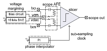
Fig 8 Scope architecture.
VII. Measurements
The DesignWare HDMI TX PHY was packaged in a wirebond 484-pin fine pitch BGA package; a die photo of the DesignWare HDMI TX PHY can be seen in Fig 9. The assembled testchip was mounted to a test board using a pogo-pin socket.
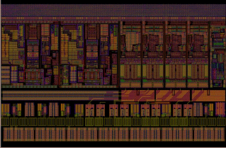
Fig 9 Die photo of the DesignWare HDMI TX PHY
The test board provided power and clocks, as well as an FPGA for configuring the PHY. The testing was performed at room temperature with typical supply voltages: VDD =1.1V, VDDA=2.5V.
The power consumption was measured over various video modes/data rates while transmitting pseudorandom data simultaneously over all 3 TX channels. These results measure the power consumed by the DesignWare HDMI TX PHY alone; the power drawn from the receiver 3.3V termination supply is not included (see Table 1).
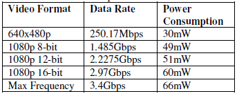
Table 1 Power consumption over video formats
Internal compliance testing was performed on the DesignWare HDMI TX PHY at the following data rates:
- 1.485 Gbps – 1080p 8-bit
- 2.2275 Gbps – 1080p 12-bit
- 3.4 Gbps – Maximum data rate specified in the HDMI specification
Rates 1 and 2 were chosen due to their prevalence in the marketplace. 1080p 12-bit is the maximum rate supported by the Sony® PlayStation®3 Blu-ray players and was identified to be the maximum rate found in the electronics market at time of development.
The following test setup was used to measure the electrical tests for internal compliance:
- Tektronix DSA70804 Oscilloscope (8GHz)
- Tektronix TDSHT3 Software
- Tektronix P7313SMA Differential Probes (13GHz) (2)
- Efficere TPA Load boards
The DesignWare HDMI TX PHY passed electrical compliance tests for all of the above mentioned video formats. Results from the 1080p 12-bit 2.2275Gbps electrical compliance can be seen in Table 2.
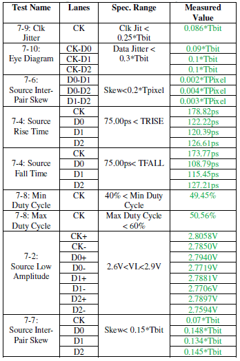
Table 2 Compliance test result summary.
The eye diagram at 2.2275Gbps and 3.4Gbps are measured and shown in Fig 10 and Fig 11 respectively. The eye diagram measured by the onchip scope is shown in Fig 12.
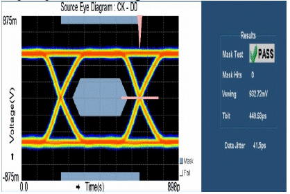
Fig 10 Source eye diagram of Ch0 – 2.2275Gbps 1080p 12-bit.
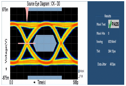
Fig 11 Source eye diagram of Ch0 – 3.4Gbps max data rate.
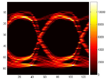
Fig 12 On-chip scope eye diagram – 3.4Gbps
VIII. Conclusion
An electrically compliant HDMI TX was designed and fabricated in a 40-nm LP process. The power consumption, jitter performance and size are among the best in the industry. Key features included: tunable source impedance, selectable transmitter pre-emphasis, independent clock and TX lane amplitude/level control, and independent clock and TX edge rate control. Several advanced analog test capabilities ease ATE evaluation at production. Finally, novel circuit topologies were used to ease the portability of this design into processes without native 3.3V devices.
Acknowledgments
The authors would like to gratefully acknowledge the Synopsys MSIP Toronto Design Team including digital, layout, hardware, PnR and CAD teams for their support during this project.
References
[1] James F. Parker, Daniel Weinlader, Jeff L. Sonntag, “A 15mW 3.125GHz PLL for Serial Backplane Transceivers in 0.13um CMOS” ISSCC 2005, pp. 412 – 414.
[2] Kannan Krishna, David A. Yokoyarna-Martin, Skye Wolfer, Chris Jones, Mat Loikkanen, James Parker, Ross Segelken, Jeff L. Sonntag, John Stonick, Steve Titus, Daniel Weinlader, “A 0.6 to 9.6Gb/s Binary Backplane Transceiver Core in 0.13um CMOS” ISSCC 2005, pp. 64 – 65.
[3] HDMI Specification v1.4
Related Semiconductor IP
- HDMI TX PHY IP
- HDMI 1.4/2.0 Transmitter PHY
- HDMI 2.0 RX PHY in SS 8LPP 1.8V, North/South Poly Orientation
- HDMI 2.0 TX PHY 6Gbps in UMC 28HPC 1.8V, North/South Poly Orientation
- HDMI 2.0 TX PHY 6Gbps in TSMC22ULP 1.8V, North/South Poly Orientation
Related Articles
- Testing the HyperTransport PHY core
- Testable SoCs : Testing the HyperTransport PHY core
- A case for using FPGAs in SDR PHY
- Making the UWB PHY a "Transparent Patient"
Latest Articles
- SoK: From Silicon to Netlist and Beyond Two Decades of Hardware Reverse Engineering Research
- An FPGA-Based SoC Architecture with a RISC-V Controller for Energy-Efficient Temporal-Coding Spiking Neural Networks
- Enabling RISC-V Vector Code Generation in MLIR through Custom xDSL Lowerings
- A Scalable Open-Source QEC System with Sub-Microsecond Decoding-Feedback Latency
- SNAP-V: A RISC-V SoC with Configurable Neuromorphic Acceleration for Small-Scale Spiking Neural Networks