SystemC Verification, Simulation & Emulation of Secure Digital IP
Contributors: Douglas Chisholm, Alan Baillie
Livingston, Scotland
Abstract:
This paper describes the process and tools used in the verification of a family of Secure Digital (SD) IP cores. The verification process described included SystemC verification, RTL simulation and emulation of the SD IP on an ARM Integrator platform.
Secure Digital is an interconnect technology which is targeted at the addition of Flash memory and IO functionality to a huge range of consumer digital products. Compliance and Interoperability testing is critical in the development of such consumer targeted products and this must be combined with a verification methodology which achieves time-to-market.
The development and context of each method of verification employed are discussed in turn and the relative merits are discussed. Recommendations of best practice are presented for developing a methodology which makes best use of simulation, SystemC verification and emulation in the design of IP targeted at consumer applications where time-to-market is critical.
Secure Digital
SD is a popular interface used to connect memory cards to digital cameras, PDAs and other hand held devices. It is becoming the dominant technology for memory cards replacing the older form-factors such as Multi Media Cards, Compact Flash, Smart Media cards.
The protocol is implemented as a 9-pin serial interface and supports up to 4 data pins. It is a synchronous interface with the clock being provided by the host device. Bi-directional command and data buses are used, implemented in a dominant-recessive manner such that the buses are pulled-high when not active. The maximum clock frequency is 25MHz and so the maximum data transfer rate is 100Mbps. Commands and data are transferred in frames with start-bit, stop-bit and CRC fields. As will be discussed in this paper the IP was seen to be sufficiently complex and have functional attributes worthy for use as a test case for exploring the different verification techniques available and their associated benefits. In particular the benefits and limitations of using a high level language, SystemC, to perform verification on non-computational IP will be discussed. The protocol is implemented in hardware and software (i.e. device driver or firmware) and as such simple Hardware Description Language (HDL) testbenches, for example using Verilog, would be difficult to develop because the required test scenarios would have to adapt to the card responses. Cadence has developed soft IP solutions for both Secure Digital Host and Card applications. The first two cores we have developed are an SDIO Host controller core and an SDIO Card controller core which supports SD IO Card applications and SD Memory Card applications – as well as multi-function card operation with IO Card and Memory Card functionality combined. Our SDIO Card controller includes optional support for C2 cipher and Authentication and Key Exchange (AKE) functionality for protection of digital content. Our SD roadmap includes support for SDMMC, Secure Digital Multi-Media Card operation.

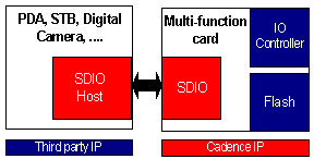
Figure 1 Cadence Secure Digital IP
Figure 1 shows examples of using Cadence IP to provide both Host and Card side SD solutions. Cadence can provide IP, Design Services and EDA Tools for companies developing Secure Digital solutions.
Standard Methodology
Traditionally HDLs such as Verilog and VHDL have been used to define both implementation and verification (testbench) IP. In general HDL testbenches are dedicated to the test of the specific core and while they can be adapted they are not always readily reusable.
Within Cadence our standard verification methodology has been based on the use of Verilog testbenches. The methodology has been developed from use over a large number of IP cores. These Verilog based testbenches make use of transactions.
Transaction based testbenches abstract the level of simulation from exercising the design under verification (DUV) at a signal level to operating at packet transfer level in terms of higher functions such as reads and writes. This results in a testbench methodology which is easier to use, faster and more readily modified than a signal level Verilog testbench.
Tests are written in easily understood commands such that users can write their own targeted tests as required. The commands are translated using Perl and Verilog into stimulus and expected results and the testbenches are portable across different simulators. The test suite is normally based on the requirements and verification specifications and standards-based checklists where these are available.
A strong positive feature of the HDL based testbenches shipped with Cadence soft IP is that they are easy for customers to understand and tailor as required. It is quite common for IP users to make small changes to the delivered core, making small changes to interfaces for example, and an easily modified testbench enables the user to reduce risk by verifying any changes that they make.
While HDL testbenches are flexible enough to be updated to verify customer design changes they are not always easily integrated into the IP user’s SoC level verification suite.
HLL Based Verification IP
There is a growing momentum in the use of verification IP developed using high level languages (HLL) such as SystemC. HLL based verification IP presents users with many advantages in terms of reuse, speed of simulation and ease of system simulation. The move to the use of HLLs has led to an increase in the availability of truly reusable verification IP which can be readily fitted into a comprehensive SoC verification strategy more readily than for RTL based testbenches.
IP and SoC developers now have the option to develop verification IP in house or source it from a growing number of third party verification IP specialists. HDL testbenches are often developed by or at least influenced by the implementation IP design team – breaking this link by using verification IP from a third party reduces the chance that the implementation and verification IPs will contain common faults.
SystemC Verification
Unified Verification Methodology
As technology moves from 0.18um and 0.15um down to 0.13um, 90nm and beyond current verification methodologies will struggle with the resultant massive increase in SoC complexity. At the 90nm process node SoC gate capacity will be more than double that of 0.13um devices, rising to over 100 M transistors. Verification complexity for register based logic rises as a square of any increase in the number of registers and so the doubling of implementation complexity will have up to a four fold impact on verification.
Traditional SoC verification methodologies have significant shortcomings – both in terms of lack of verification reuse throughout the design-proving process and in terms of software validation being heavily dependent on the availability of proven hardware. The additional verification complexity of SoCs with over 50 M gates makes fragmented verification methodologies intolerable.
This verification time bomb has led Cadence to create the unified verification methodology (UVM). The UVM utilises transaction level modeling and hardware acceleration in a platform which enables the co-coordinated verification of all aspects of the design: embedded software, control, datapath, analog, mixed-signal and RF. The implementation of the concepts of the UVM in the Incisive verification platform makes verification reuse a reality.
Verification reuse is supported through the definition of the Functional Virtual Prototype (FVP). The FVP leverages transaction level modeling so as to enable hardware and software design proving to progress without the requirement for RTL verification to be complete. By supporting a building block approach which starts with a transaction based FVP and progresses to switch in RTL cores as these become available, the UVM enables SoC developers to move verification forward in a parallel manner and in doing so cuts verification time by up to 50%.
In this paper we will be describing the use of transaction level modeling in the design proving of a Secure Digital IP core. The SD core is not being implemented into a complex SoC, however the development of a transaction level model for this core will enable Cadence customers to develop FVPs for their SoCs and take advantage of the significant verification benefits discussed above.
Transaction Level Modeling
Transaction level modeling raises the level of abstraction of simulation through replacing signal level events with higher level operations such as reads and writes. By raising the level of simulation abstraction it is possible to benefit from speed improvements of up to x100 compared with RTL level simulation.
The project demonstrates the development of a transaction level model (TLM) of the Cadence SDIO Card IP core, the use of this in simulation followed by replacing the TLM with the RTL version of the core when this becomes available.
Verification methodologies which combine transaction level models with RTL descriptions of design blocks face the difficulty of supporting communication between blocks which are described using different levels of abstraction: the TLM working at a packet transfer level, carrying out reads and writes, while the RTL works at the interface signal level. The transactions to signals communications mismatch is handled by the ‘transactor’ function – this behaves as a data level translator, decoding reads and writes into the related signal activity and vice versa.
FVP with TLM
The TLM consists of a model of the SDIO core written in SystemC. This describes the function at a transaction level, describing transfer structures which contain data plus control and status information. The model is event driven, not clocked as would normally be the case for an RTL implementation.
In a standard application the SD core would be driven by an SD Host – and this is implemented through the creation of a transaction level traffic generator which acts as master when running tests. TLMs require the combination of master and slave traffic generators in order that transactions can be initiated and responded to. TLM traffic generation defines various categories of traffic – in this case the master allows transactions to be generated either in a directed manner or using constrained randomisation. Directed traffic is clearly defined and represents obvious transfers that are readily identifiable. The generation of random traffic provides an automated way of improving the code coverage and functional coverage of the design.
Constraints are applied as part of the process to control, for example, the ratio of valid to invalid command sequences and data values.
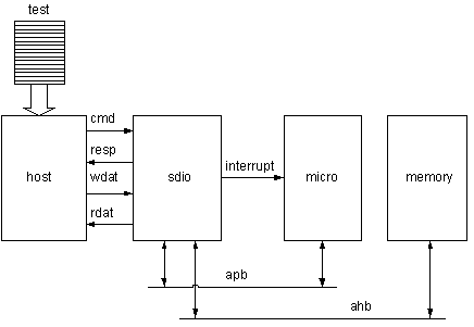
In a similar fashion the SD would normally be controlled by an embedded processor such as an ARM for example. In our TLM a simple microprocessor model is described and this is used to configure and control the SD module. The microprocessor model programs the SD core via its APB interface. It responds to interrupts from SD module, using interrupt handler code written in C.
The components of the TLM were validated using the test setup shown in Figure 2. The block marked memory is implemented as a simple transaction level behavioral model.

Figure 2 Proving the SDIO TLM
FVP with RTL
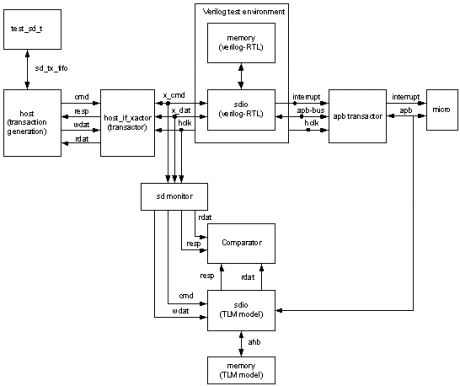
Having completed testing of the SDIO TLM, transactors were developed to convert between the transaction level model interface and the Verilog signals of the RTL. In this case three transactors were required, one for each of the Host and APB interfaces to the TLM , plus one to reconstruct transactions as part of the automatic response checking mechanism.
The Host I/F transactor was developed to convert between traffic generator transactions and bidirectional Verilog signals. This converts command and write data transactions to Verilog serial command and data bitstreams. For flow control handshake purposes, the transactor constructs response and read data transactions by monitoring Verilog serial bitstreams.
The APB I/F transactor was developed to convert between the microprocessor model transactions and the signal level interface presented by the Verilog implementation of the APB.
The third transactor, the monitor, analyses the input signal activity on the RTL host interface to construct corresponding transaction inputs to the SDIO TLM. It also constructs transaction level equivalents of the responses from the RTL and passes these to a transaction comparator. The second set of inputs to the comparator is provided by the TLM. This combination of monitor, TLM and comparator therefore forms the response checker for the testbench. Any mismatches between actual responses from the RTL and those expected by the TLM are detected by the comparator and reported to the user.

Figure 3 – Proving the SDIO RTL
Transaction viewing
Figure 4 shows command and response transactions with the corresponding Verilog signal activity. This was taken from the Simvison waveform viewer.

Figure 4 Signal and transaction level activity
The Incisive platform allows device under verification (DUV) activity to be displayed at transaction level. In the example waveform shown in Figure 4 it can be seen clearly that signals and transactions can be viewed together in the Simvision waveform viewer – this is very useful for testbench development and also for ensuring confidence in the operation of the transactors.
Transaction fields provide higher level interpretation of signal activity – making debug of device operation more straightforward and hence faster.
Transaction level testbenches are suitable for generation of random traffic as well as protocol checking. In addition FVPs can be used in architectural exploration, for example using TLM modeling to determine optimum buffer sizes. In such a case the ability to quickly change models and rerun simulations is a major benefit.
Emulation
FPGA based emulation may not be suitable for every application – for example some high speed digital cores will not operate at full speed when synthesized to FPGA and the process specific aspects of hard IP make them unsuitable for FPGA emulation. However for a great many cases FPGA emulation is extremely useful. It can be the quickest and simplest way to prove IP in silicon and avoids the pain of large non-recurring engineering (NRE) costs associated with mask development for ASIC and SoC applications.
Of particular value is the opportunity to make changes to the design in real time. This can be useful, for example, when taking test silicon to compliance and interoperability testing. FPGA based emulation enables progress through a series of problems by supporting a repeated process of testing, fixing and retesting.
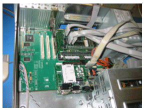
At Cadence we have a lot of experience in using ARM Integrators, which are excellent for the development of AMBA based IP cores. ARM Integrators provide ARM infrastructure into which AMBA based IP can be readily integrated and quickly tested. Figure 5 is a picture of our ARM Integrator based Secure Digital test environment.
During the development of our SD Host Controller we were able to carry out interoperability testing of the IP core within hours of synthesizing the core to FPGA. Likewise in this project where we are looking to test the SDIO Card controller the ARM Integrator significantly reduced the effort to carry out emulation. FPGA emulation enabled the testing of real-time behaviour such as time-outs and supported simple software development.
FPGA based testing is much quicker, allowing exhaustive testing to be carried out significantly faster than in simulation. The use of real traffic in testing is very useful, in this case connecting our SDIO Card controller to a real SD Host.
As we were developing both Host and Card solutions we were able to benefit from simulating these together and testing them together in FPGA. This was carried out after the Host had been through interoperability testing with leading 3rd party SD Memory Cards.
The debug of our SD IP cores on an ARM Integrator, shown in Figure 5, was particularly beneficial as it was possible to run the cores at full speed.

Figure 5 Debug and Interoperability Platform
Conclusions
The paper has described the verification strategy used in the development of the Cadence SDIO Card controller IP. The development of the FPGA platform has been useful in accelerating design debug and in early interoperability testing – it will also form the platform for carrying out formal Compliance and Interoperability testing in future.
The use of an FVP had significant value in accelerating design verification and in providing a baseline against which the RTL implementation could be verified. In addition the methods used in proving the IP can be readily reused in customer SoC developments – providing genuine reusability of verification platforms and IP.
There was a learning curve required for members of the team for whom this was the first project in which they used SystemC – and this learning exercise will not be uncommon for companies whose engineers are more familiar with the use of HDLs such as Verilog and VHDL than higher level languages like SystemC. However having been through this process once the engineers felt that the learning exercise was well worth the overhead as the benefits of using transaction level modeling outweighed the learning costs.
For the development of our SD IP, complex digital IP targeted at the fast moving consumer market, the combined use of TLM and RTL based modeling followed by FPGA emulation has improved verification speed and quality as well as enabling Cadence to offer additional value to our IP customers.
Related Semiconductor IP
- Bluetooth Low Energy 6.0 Digital IP
- Ultra-low power high dynamic range image sensor
- Flash Memory LDPC Decoder IP Core
- SLM Signal Integrity Monitor
- Digital PUF IP
Related White Papers
- How formal verification saves time in digital IP design
- Formal-based methodology cuts digital design IP verification time
- Out of the Verification Crisis: Improving RTL Quality
- Rapid Validation of Post-Silicon Devices Using Verification IP
Latest White Papers
- How Next-Gen Chips Are Unlocking RISC-V’s Customization Advantage
- Efficient Hardware-Assisted Heap Memory Safety for Embedded RISC-V Systems
- Automatically Retargeting Hardware and Code Generation for RISC-V Custom Instructions
- How Mature-Technology ASICs Can Give You the Edge
- Exploring the Latest Innovations in MIPI D-PHY and MIPI C-PHY