System Test using JTAG
Chintan Panchal, Parth Rao (Einfochips)
Abstract:
Boundary Scan technique is most often thought of as a board-level test method, but certain techniques makes system level test with JTAG quite effective. Many types of faults can arise when systems are assembled. JTAG testing techniques are well suited to finding and diagnosing many of these problems. For example, a connector may not be making good electrical connect or a connector’s pins might be damaged during assembly, some parts of device might be missing or not functioning properly. This paper will show the certain techniques like “Ring Architecture”, “Star Architecture” and “Multi-drop Architecture” for System level test using JTAG. Though the JTAG IEEE 1149.1 standard is widely used for board level test, this paper would show the applications of the same standard at the system level test. The system level test using JTAG techniques can be very helpful to support and maintenance personnel long after a system has been assembled in a manufacturing environment and installed at a customer location.
I. INTRODUCTION
What is system test and why would you want to do it?
To begin the discussion of System level testing using JTAG standard, certain basic aspects of system test must be cleared like what is system test and how it is distinguished from board level test. A system can be defined as “a group of interrelated, interacting, or interdependent elements forming a complex whole” [1]. System can be simply defined as the connection or combination of more than one board, to accomplish certain task. This could be an assembly as simple as a mother/daughterboard combination or an extremely complex backplane-based computer with hundreds of boards. So, with the help of this definition, it can be said that an electronic system is a group of interconnected devices and boards that function together to accomplish a task. The basic goal of system test is to verify the structural integrity and/or functionality at the level of the complex whole, though the components that comprise an electronic system may be tested individually without regard to the task of the entire system. At a fundamental level, testing a system’s structural integrity means to verify that each component is properly connected to all other components that require such connections.
II. DFT TECHNIQUES
Why systems test?
Most electronic products can be seen as a system. Even if all of the system’s components are fully tested individually, the system still may not function properly. Many problems can arise when systems are assembled. Boundary scan techniques can provide the possible solution to find out and diagnose these problems. For example, a connector may not be making good electrical contact or a connector’s pins might be damaged during assembly. Boards on a backplane may be missing, out of place or simply not functioning properly. Functional tests can identify that the system is not functioning as per the expectation, but isolating and diagnosing the fault with functional tests would be very time consuming and often would require high level system expertise to troubleshoot the cause.
In addition, boundary scan techniques can also perform various operations apart from the test functions. Besides structural integrity tests, boundary-scan can also perform on-board programming of flash memory, in-system configuration of PLDs, on-board programming with I2C data and emulation-based functional testing through a processor’s JTAG debug port. Beginning with system-level debug and production test, boundary scan provides many other system benefits when it is extended to field support. For example, boundary scan can be used for quick and easy updates of programs stored in flash memory or updates to system functionality in the field through the re-configuration of on-board PLDs [2].
III. ARCHITECTURES
How is system test implemented with boundary scan?
Three primary methods are available for implementing boundary-scan-based system tests. All of these methods involve connecting an external boundary-scan test tool to the system.
Ring Architecture:-
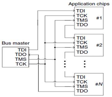
The first external method connects all of the boundary scan paths on all of the boards in the system to a single scan path with one point of access for the boundary scan test system (Figure 1). This method requires that the configuration of the system must remain exactly the same in every assembled product. Also, any break in the single scan path will disable all boundary-scan test access. One very long scan path can also result in slow access times.

Fig. 1: Ring Architecture [3]
Star Architecture:-
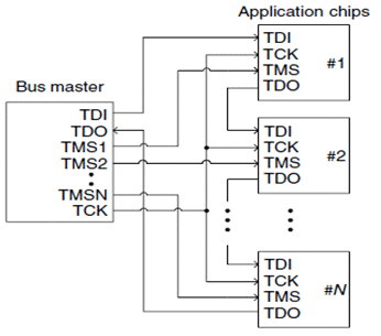
The second method of testing system is the star architecture. In a backplane star configuration as shown in figure 2, the backplane drives TCK and TDI directly to all boards and each board outputs a TDO signal to the backplane. Each board requires a unique TMS signal from the backplane and a separate circuit trace for each signal. During testing, only one board is enabled at a time and only the TMS signal for that board is active. With this architecture, virtually all chips can be tested independently. STAR configuration is used to test the connectivity between IC and PCB and its separate functionality at a time.
The advantage of the ring and star architectures is that they do not require any additional components or new protocols beyond what is required by the boundary-scan specification. This makes them straightforward to implement, but in a large multiple-board system they are often too cumbersome to use [3].

Fig. 2: Star Architecture [3]
Multi-drop Architecture:
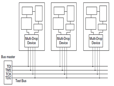
The third method is to design a method for controlling access to the scan paths on the individual boards from one external JTAG port (Figure 3). A multi-drop gateway device must be inserted on the board which controls the board for the purpose of testing system. A multi-drop architecture uses only one set of 1149.1 data and control signals which is wired in parallel to each board in the system. An addressable gateway device must be implemented on each board, to ensure that boundary-scan operations are applied to only one board at a time. A special selection protocol is applied to the boundary-scan bus by the system-level boundary-scan controller to connect the chosen board’s scan chain to the bus. This solves the problems mentioned above (in Ring and Star configuration) at the expense of extra selection logic in each board.

Fig. 3: Multi-drop Architecture [3]
There are commercially available multi-drop gateway devices, including the following:
- Texas Instruments
- Scan Path Linker (SPL) – SN54ACT8997
- Addressable Scan Port (ASP) - SN54ABT8996
- Linking Addressable Scan Port (LASP) – SN54LVT8986
- National Semiconductor
- Scan Bridge (SCANSTA111, SCANSTA112)
- Firecron (Alliance Semiconductor)
- Gateway (JTS03, JTS06)
- Lattice Semiconductor
- BSCAN2 (Multiple Scan Port Linker)
Several methods are available for controlling multi-drop devices and the secondary scan paths associated with them. In some cases, a certain scan path configuration may be needed for several test operations. Or, the scan path may be dynamically reconfigured before an action can be applied. In either case, a particular scan path configuration would be maintained until it is explicitly changed by the Scan Works or until a JTAG Test Logic/Reset operation occurs.
The table below provides a summary of the advantages and disadvantages of the three system-level test methods [2].
| Method | Advantages | Disadvantages |
| Star Architecture | Simple, single point of access | One break in the scan chain will disable all boundary scan operations. Slow access times. |
| Ring Architecture | It is used to test the connectivity between IC and PCB and its separate functionality at a time. | Multiple TMS lines significantly increase the backplane signaling [4]. In a large multiple-board system they are often too cumbersome to use. |
| Multi-drop Architecture | Tests are controlled by multi-drop gateway devices. Straightforward interface with test system. | Gateway devices require board or backplane space and add to the cost of the system. Each system configuration requires its own test suite. |
IV. CONCLUSION
Boundary Scan testing has established a strong position in the board level testing. As more and more board-level boundary scan tests are developed, the feasibility of implementing system level test using JTAG (Boundary Scan) techniques increases because of the requirement of testing at the system level. It is important that the board and system designers are aware of the benefits and effectiveness of extending the IEEE1149.1 standard in a system test environment. The architectures discussed in this paper have been readily adopted by the leading silicon vendors of the system test access devices so that the system architects have far more flexibility in implementing the system level test strategy. So this would be considered as solutions to the system level testing.
REFERENCES
[1] Wordnet Dictionary
[2] ASSET Whitepaper : system Test with Boundary Scan (JTAG)
[3] VLSI Test Principles and Architectures Design For Testability, Laung-Treng Wang, Cheng-Wen Wu, Xiaoqing Wen
[4] Design Considerations In Using 1149.1 As a Backplane Test Bus, Pete Collins, petec at jtag.co.uk, JTAG TECHNOLOGIES
Related Semiconductor IP
- ReRAM NVM in DB HiTek 130nm BCD
- UFS 5.0 Host Controller IP
- PDM Receiver/PDM-to-PCM Converter
- Voltage and Temperature Sensor with integrated ADC - GlobalFoundries® 22FDX®
- 8MHz / 40MHz Pierce Oscillator - X-FAB XT018-0.18µm
Related Articles
- System on Modules (SOM) and its end-to-end verification using Test Automation framework
- Boundary scan and JTAG emulation combine for advanced structural test and diagnostics
- System Performance Analysis and Software Optimization Using a TLM Virtual Platform
- ACE'ing the verification of a cache coherent system using UVM
Latest Articles
- Quantifying Uncertainty in FMEDA Safety Metrics: An Error Propagation Approach for Enhanced ASIC Verification
- SoK: From Silicon to Netlist and Beyond Two Decades of Hardware Reverse Engineering Research
- An FPGA-Based SoC Architecture with a RISC-V Controller for Energy-Efficient Temporal-Coding Spiking Neural Networks
- Enabling RISC-V Vector Code Generation in MLIR through Custom xDSL Lowerings
- A Scalable Open-Source QEC System with Sub-Microsecond Decoding-Feedback Latency