Silicon IP for Programmable Baseband Processing
Linkoping, Sweden
Abstract
An efficient IP reuse strategy relies on IP blocks with wide applicability. That makes generic blocks, such as programmable processors preferable. However, in many applications such as handheld wireless terminals, additional silicon area and power consumption compared to fixed function solutions can not be accepted.
In this paper it is shown that an application specific instruction set processor can meet the requirements on flexibility and power consumption while reaching a smaller silicon area than a nonprogrammable solution.
As an example Coresonic’s LeoCore architecture is presented. LeoCore uses a new type of instruction set architecture which exploits the computational properties of baseband processing applications. This leads to large parallelism and efficient hardware reuse with low control overhead and very high code density for baseband applications.
1 Introduction
Silicon reuse is the key solution in modern system on chip design (SoC). Themain motivation to this is of course a substantial reduction in design and verification time of a new product, by utilizing blocks that are already verified. An efficient reuse strategy requires IP blocks with wide applicability. Therefore generic blocks, as for example processors are preferable. In the same time we can not accept any silicon area or power consumption penalty compared to a tailored solution.
In this paper we will show that application specific instruction set processors not only fulfill the basic requirement above to have a wide applicability, but also meet the area and power constraints.
We will show that replacing a tailored solution by a processor solution we save considerable silicon area by the reuse of computing and control resources. By further recognizing that most tailored solutions are used for deterministic problems, we can remove unnecessary flexibility from the processor, thus considerably reducing the control overhead. Resource reuse, together with a simplified control overhead also allows the elimination of the power consumption penalty commonly occurring in programmable solutions.
To illustrate our point we use a concrete example, an application specific instruction set processor aimed at wireless modem functions and covering all wireless standards. This example fulfills the requirements above of being generic in relation to a large number of applications and replacing many tailored solutions of today.
Regarding the wireless market several benefits from programmability can be listed:
-
Reuse of the same hardware platform in different products and applications.
-
Shorter development time (just new software instead of new hardware).
-
Adaptability to new and changing standards.
-
Wireless download of new features and software patches.
-
Extensive use of hardware multiplexing leading to reduced silicon cost for multi mode devices.
Contrary to popular belief, it is possible for a programmable solution to achieve smaller silicon area than a fixed function solution even for a single standard [1, 2]. This is due to the fact that a programmable solution can reuse the same hardware not only between standards but also between different parts of the processing flow, something which is difficult to achieve in an ASIC. In addition, by carefully exploiting the right trade-off between flexibility and performance, it is possible to avoid power penalty over fixed solutions.
2 Architectures for Programmable baseband
Figure 1 gives an overviewof the baseband processing flow.
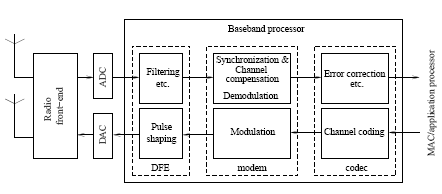
Figure 1: The baseband processing flow
-
The digital front-end (DFE) contains per sample operations such as filtering, DC-offset cancellation, and frequency offset compensation performed on all incoming samples.
-
The modem performs the modulation and demodulation as well as functions such as synchronization, channel estimation and equalization. The operations involved is to a large extent operations on vectors of complex-valued samples (I/Q-pairs) such as correlation, vector multiplication, and FFT.
-
The codec performs bit-based operations such as scrambling, interleaving and error correction (Viterbi, Reed-Solomon etc).
Out of these three parts, the modem is the one that benefits the most from programmability. This has several reasons:
-
Convolution based operations such as correlation and FFT can be efficiently implemented on programmable DSP processors with MAC units and support for convolution based processing. Bit based operations on the other hand are in general rather tedious to implement in software but often have very efficient hardware implementations, such as linear feedback shift registers. The relative overhead for instruction fetching and decoding is much smaller for an instruction doing a FFT butterfly than for an instruction doing a small bit manipulation operation.
-
The modem stage is the part showing the most diversity between standards and also the place showing themost development in terms of new modulation schemes. For the DFE and codec stages on the other hand a limited set of functions are required to support most standards and a relatively low degree of configurability is sufficient.
-
The modem is the place where a manufacturer has freedom to differentiate their product from competitors by improving algorithms to increase performance.
Coresonic’s design philosophy can be summarized in two bullets:
-
Start from application, not from architecture.
-
Find the right flexibility.
The first bullet implies that taking an existing architecture and adapting it for your application is probably not the right approach. Instead your first step should be to carefully characterize the properties of your application. This includes not only to profile the operations involved but also for example data types and precision requirements, real-time requirements, data access patterns, control complexity, and data dependencies.
Baseband processing differs from general computing in many ways. On one hand, baseband processing is a hard real time problem posing heavy computational demands and large amounts of data combined with latency requirements on the 1 ìs scale. On the other hand the control flow is predictable and there are few data dependencies. The real-time requirements make predictable execution time essential for an efficient baseband processor. At the same the possibilities for parallelization through vectorization (SIMD) and function level pipelining enabled by the absence of data dependencies should be exploited. Some properties of baseband processing are listed in table 1.
The art of designing application specific processors consists to a large extent of finding the right trade-off between flexibility and performance. Performance can be reached either through application specific acceleration or general architecture enhancements, as illustrated in Figure 2.
Similarly the memory bandwidth required can be reached through wider memories, more memory banks, or by using multi-port memories, Each solution representing a different flexibility verses cost trade-off.
To make the right choices it is necessary to posses in-depth application knowledge as well as a well developed methodology for evaluation of different architecture configurations.
3 Existing Architectures
Various programmable architectures dedicated for baseband exist today. Many of these, such as Sandbridge’s Sandblaster architecture [3], Philips’ OnDSP and EVP16 [1] and Silicon Hive’s Avispa- CH1 [4] are based on more or less traditional VLIW or VLIW/SIMD combinations. Sandblaster combines this with a multi-threading scheme while OnDSP and EVP introduces a vertical code compaction scheme to exploit the vector processing characteristics of baseband applications. Less traditional architectures are provided by Icera’s [5] Deep Execution Processor concept and Morpho Technologies [6] configurable data path.
Table 1: Baseband application characteristics
| Data types | Large portion of complex-valued computations,moderate to low precision requirements |
| Real-time requirements | Hard real time, very tight latency requirement |
| Data access | High data rate but predictable access patterns and large locality |
| Control characteristics | Low complexity, few data dependencies |
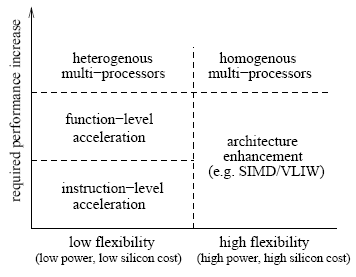
Figure 2: Means to increased performance
Yet another approach is the heterogenousmulti processor solution from Picochip [7].
Philips and Silicon Hive relies on hardware acceleration for DFE and codec functionswhile Sandbridge and Icera aims at running everything in software. Out of the abovementioned architectures the ones from Silicon Hive and Morpho are offered as Silicon IP.
4 The LeoCore architecture
As indicated above, the preferred approach to an efficient baseband architecture is to start with a careful characterization of the application. This approach was used when developing the LeoCore architecture [2, 8]. The space does not allow a complete description of this process, instead we chose to describe the architecture below, and motivate some of the architectural choices made.
4.1 Architecture Overview
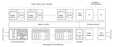
Figure 3 gives an overview of the LeoCore architecture. A network structure is used to interconnect memory blocks, vector execution units and accelerators. The structure can be roughly divided into two parts. The first part handles modem functions based on complex-valued data. This is mostly handled by SIMD execution units. The second part is scalar or bit based operationsmuch of which is handled by accelerators. A small RISC-style execution unit handles control flow, integer arithmetics, and network and accelerator configuration.
4.2 Complex Vector Processing
The LeoCore uses a new type of instruction set architecture which we have chosen to call “Single Issue Multiple Tasks”, or in short SIMT. The architecture relies on the observation that most baseband processing tasks operate on a large sets of complexvalued vectors.
The bulk of the modem processing is handled by SIMD execution units. In addition to being optimized for operations on complex-valued vectors, these units provide instruction level acceleration of important baseband functions such as synchronization, FFT, and CDMA despread/RAKE.
The important new feature of these units is the vector execution control blocks which handle a novel type of vector instructions that operate on vectors of arbitrary size (i.e. not limited by the SIMD data path width). This allows operations such as a scalar product between two complexvalued vectors or one layer of an FFT to be coded by a single short (16 to 24 bits) assembly instruction.
The most important characteristic of the SIMT instruction set architecture is illustrated in Figure 4: The idea is that only one instruction is issued each clock cycle, but several vector instructions and control instruction can run in parallel. This approach results in a degree of parallelism equivalent to a VLIW machine but with smaller control path and much higher code density. Even compared to the most efficient code compaction schemes for VLIW, the code size is reduced by approximately a factor two.
4.3 Memory organization
Another important characteristic the SIMT scheme is that data memory address generation is independent from the instruction decoding and control path. This is achieved by using several decentralized memory blocks, each with their own associated address generation units (AGUs). Decentralized addressing also eliminates the need for communicating addressing information over the network.
Click to enlarge
Figure 3: LeoCore architecture overview
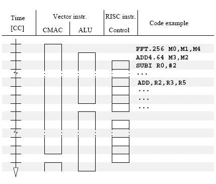
Figure 4: The SIMT principle
A significant memory bandwidth, in the order of several hundred bits per clock cycle, is needed to keep the vector SIMD units occupied during regular processing. Memory bandwidth is increased by using interleaved single port memory banks. This means that consecutive elements in a vector always can be accessed in parallel even without the need for multi-port memories. In addition to linear vector addressing and modulo addressing, some of the memory blocks have a FFT addressing mode handling bit reversed addressing and avoiding memory access conflicts during FFT execution.
4.4 The Network
The network is also an essential part of the memory system. Using a crossbar-type interconnect scheme under full software control eliminates the need for arbitration and addressing logic, thus reducing the complexity of the network and the accelerator interfaces. It also provides low latency, many simultaneous connections and complete predictability. An execution unit or accelerator always has exclusive access to a memory. Thereby stall cycles due to memory conflicts are eliminated. After completion of a task the entire memory containing the result can be “handed over” to another unit by reconfiguration of the network. Thereby data moves between memories are avoided.
In addition to assuring efficient use of data memory the network also allows flexible and efficient integration of accelerators with minimized communications overhead. Via the network the set of accelerators used in the currentmode of operation can be connected into a chain. Once such a chain has been set up, data is transfered between accelerators without any interaction fromthe controller. The need for DMA features and for intermediatememory storage between accelerators is also avoided.
4.5 Benchmarks
Currently two implementations of the LeoCore architecture is under development. The first, LeoCore-1, is aimed at applications such asWLAN IEEE 802.11a/b/g, GSM, Bluetooth, DVB-T and lighter WiMAX modes. It has a double complex MAC unit capable of for example two complex-valued multiply-accumulate operations or one radix-2 FFT butterfly per clock cycle.
A prototype chip handling the complete 802.11a and b digital PHY, with the exception of the 11a Viterbi decoder, was taped out in a 180 nm process. The silicon area was 2.9 mm2 including core, accelerators, and enough memory to keep both applications on-chip simultaneously. During 11a packet reception peak power was measured to 120 mW running at 160 MHz, or 0.75 mW/MHz.
With the second generation processor, LeoCore- 2, DVB-H, mobileWiMAX andWCDMA is added to the list of supported standards. This core has a 4-way complex MAC which also does one radix- 4 FFT butterfly per clock cycle. A 4-way complex ALU providing instruction level acceleration for WCDMA despread and RAKE processing has also been added as well as some addressing support for RAKE processing. Finally the controller core has been enhanced with an integer MAC unit. A first LeoCore-2 prototype chip will be taped out late 2006. Including enoughmemory to run DVB-T andWCDMA, but without forward error correction accelerators the silicon area is estimated to 10 mm2.
Table 2 shows benchmarks for the two cores.
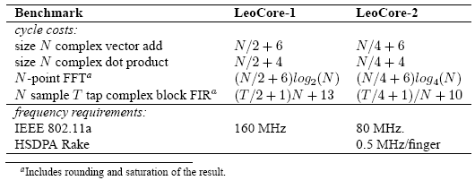
Table 2: LeoCore benchmarks
5 Conclusion
We have demonstrated that a programmable solution optimized for a specific application domain can reduce silicon area as well as reach competitive power figures compared to fixed function solutions for wireless applications. From an IP reuse perspective this is of particular interest since it enables the creation of powerful and efficient IP blocks which can be reused in a wide variety of applications.
Coresonic’s LeoCore programmable baseband cores employ the innovative SIMT principle. Relying on the large fraction of vector based operations present in baseband processing it achieves a high degree of parallelism combined with low control overhead and very compact assembly code. The architecture also allows efficient integration of hardware accelerators for carefully selected functions.
Measurements on prototype silicon indicates that this may be the first programmable architecture that can truly compete with the power consumption of fixed function solutions.
References
[1] Kees van Berkel et.al, Vector Processing as an Enabler for Software-Defined Radio in Handsets from 3G+WLAN Onwards, proc. SDR Technical Conference, November 2004.
[2] Eric Tell, AndersNilsson, and Dake Liu, A Programmable DSP core for Baseband Processing, proc. of IEEE North EastWorkshop on Circuits and Systems, July 2005.
[3] http://www.sandbridgetech.com
[4] http://www.silicon-hive.com
[8] Anders Nilsson, Eric Tell, and Dake Liu, Design Methodology for memory-efficient multistandard baseband processors, proc. of Asia- Pacific Communication Conference, October 2005.
Related Semiconductor IP
- NPU IP Core for Mobile
- MSP7-32 MACsec IP core for FPGA or ASIC
- 100G / 200G / 400G / 800G / 1.6T MACsec
- 32 bit RISC-V Multicore Processor with 256-bit VLEN and AMM
- UHF RFID tag IP with 3.6kBit EEPROM and -18dBm sensitivity
Related White Papers
- DSPs duel FPGAs for 3G baseband processing chores
- Can tools keep up with programmable silicon?
- Programmable network processing blade needed in switching platform
- Multi-Ports Eliminate Baseband Processing Bottlenecks
Latest White Papers
- Concealable physical unclonable functions using vertical NAND flash memory
- Ramping Up Open-Source RISC-V Cores: Assessing the Energy Efficiency of Superscalar, Out-of-Order Execution
- Transition Fixes in 3nm Multi-Voltage SoC Design
- CXL Topology-Aware and Expander-Driven Prefetching: Unlocking SSD Performance
- Breaking the Memory Bandwidth Boundary. GDDR7 IP Design Challenges & Solutions