Securing Smart Connected Homes with OTP NVM
By Jingliang Li, ASIC Architect, IoT Department, Synaptics
and Krishna Balachandran, Product Marketing, NVM IP, Synopsys
Introduction
The smart, connected home vision is close to reality. Imagine the following scenario.
You get a camera notification on your phone that the Grade AAA Sichuan Whole Peppercorns that you ordered have arrived. This is because your smart home camera recorded the delivery of the expected package, read the bar code, and traced it back to your online order. You come home from work and the camera recognizes you and opens the door for you. When you enter the kitchen, you find that the display on the refrigerator shows that you have enough organic fresh tofu and fresh green onions to cook ma-po tofu. Before you begin cooking, you refresh your memory of the recipe by asking your voice assistant, which reads out the steps after an online search. Just as you finish cooking, you hear from your voice assistant that your partner is home. That is because the Smart Camera recognized your partner at the door and broadcast it to all your connected home devices, which your voice assistant picked up and communicated to you. You decide to play mood music to relax and ask your voice assistant to search for contemporary jazz artists from your online music subscription, which then blankets your dining room until dinner is over. Next you watch your favorite late-night comedy show, by asking your set-top box to switch to the appropriate channel. Right before bed, you study your appointments on the smart display and ask it to wake you up a couple of hours before your first meeting. Then you close your eyes, the lights slowly dim and turn off, and a night light switches on in case you need to get up in the night.

Figure 1: Vision of the smart connected home, which is fast becoming a reality
The scenario depicted above is close to reality and a privileged few can enjoy such a smart, connected home today. This has been made possible by the confluence of processing, communication, voice and image recognition, and artificial intelligence technologies. The connected home comprises of smart home devices that process information, communicate with each other, recognize voice commands, display information, and act with each other in cohesion. This is truly the manifestation of the Internet of Things (IOT), poised to change the way we live, forever.
Smart Home Devices Need Lots of Smarts
Semiconductor companies are focused on creating powerful smart home devices to usher in the promise of the smart, connected home. These devices are realized as systems-on-chip (SoCs) designed to meet the sustained performance requirements for different use-cases and optimized for recognition of far-field voice commands.

Figure 2: Typical smart connected home SoC
Sustained performance is achieved by harnessing the combined processing power of central processing units (CPUs), graphics processing units (GPUs), and neural network engines. For example, optimization for far-field voice communications involves the ability to recognize and distinguish voice commands from background noise or sounds emanating from media players. A neural network engine is employed in parallel to the processors to endow the edge devices with intelligence to execute application such as voice recognition and natural language processing, event detection, and object recognition, all of which learn from the user preferences. Appropriate interfaces need to be integrated into the smart home devices to enable them to communicate with each other. As some of the devices will be plugged into the wall and others will be battery operated, designing for low power is a requirement. Finally, the devices must be equipped with proper firmware and software to enable seamless support for enterprise and service providers.
Though smart home devices can communicate with centralized servers and benefit from the processing power of enterprise cloud computing, latency can get in the way of fast response times—for example, turning on the sprinklers, if fire is detected in the house, needs to happen fast. For situations like this, devices need some level of edge intelligence, so stacking a host of processing capabilities in these devices is the preferred choice of smart home device vendors.
Security and Privacy are Critical to the Smart, Connected Home
Smart home devices handle a lot of your private data, such as your biometric information, as well as copyrighted media and data. Securing private data is critical--so critical that in September 2018, California passed a cybersecurity law mandating the security of connected devices. The law will go into effect in 2020 and requires IOT device manufacturers to equip reasonable security features in all internet-connected devices. Data privacy is at the center of why many users don’t want to have their information sent to the cloud for processing. Report after report from third party companies testing security of connected smart home devices have revealed serious privacy flaws in their security implementations. Findings included vulnerabilities in authenticating the users and open backdoors when communicating with the vendor’s cloud service. Privacy scandals have even included service providers recording and analyzing private conversations between the residents of a home. A cybercriminal trying to harvest personal data for identify theft can exploit the many vulnerabilities and create spearfishing attacks to gain access to user accounts.
The privacy problem is further exacerbated with the need to store and process more data at the edge, which is the preferred choice of smart home device developers to deliver low latency and fast response times. Edge devices can be even more prone to attacks than central servers in the cloud. While cloud servers are managed by large companies with lots of resources and their reputations at risk, edge devices can and do come from vendors with varying degrees of commitment to security in favor of smaller form factors, lower costs, or faster time-to-market. The increasing amounts of personal and private data stored in edge devices can be a treasure trove for hackers.

Figure 3: Examples of valuable assets in smart home products can include copyright-protected content and biometric data
Valuable Assets in Smart Home Products
There are several valuable assets that warrant privacy protection in smart home products. Video and audio programming are copyright protected and streamed content is usually available only with a paid subscription. Conditional access, based on user authentication, is used to prevent unauthorized access to copyright-protected media. Unique product information (such as chip identification, version number, authorized market segments, and product configurations) is often used to determine who has access to which devices and content and need to be protected as well. Without protection, the unique product information can be used to impersonate the product to gain access to copyright-protected information. Smart home devices gather user data such as fingerprints, voice and face identification data, payment information for paid services, and personal health data, all of which are very sensitive and private. Finally, the product maker’s intellectual property stored in the smart home device, such as source code and program data, also needs to be protected.
Types of Attacks on Smart Home Devices
Attacks from cyber criminals can take many forms. The hacking event can lead to a remotely disabling a connected home device, identity theft from eavesdropping on the user data stream, exfiltrating protected content, or re-purposing the functionality of a smart home device. Exfiltrating protected content such as audio and video programming is common and leads to copyrighted material being pirated and made available for unauthorized access. In a typical attack, the hacker targets a smart home device’s neural network algorithms that process voice or perform facial recognition. The hacker proceeds to first reverse engineer the software or algorithms and then insert malicious modifications to achieve alternate functionality or performance. Hackers with physical access to the devices can perform attacks that extract encryption keys, critical instructions, critical data, and device maker’s intellectual property.
Designing SOCs with a Security Mindset
The semiconductor industry has been diligently working to secure smart home devices and come up with the concept of a Trusted Execution Environment (TEE) to ensure secure, smart, connected home devices.
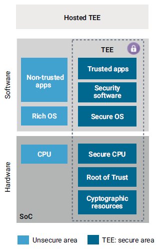
Figure 4: Trusted Execution Environment (TEE) within an SoC enhances security
The concept of a TEE is straightforward—create a trusted platform of hardware and software to ensure protection of code and data. The goal of a TEE is to maintain authenticity, integrity, and confidentiality of the system. Authenticity ensures that the system behaves as expected and correctly protects the sensitive assets. Authenticity is achieved through a chain of trust built on a Root of Trust embedded in SoC hardware. Integrity prevents modification of authenticated code and data during the SoC code execution time. Confidentiality prevents code and data from being exported out of the device without proper authentication. Confidentiality is achieved by using encryption keys to protect sensitive data. Encryption keys are derived from the Root-of-Trust keys securely stored in SoC hardware.
Designers can take multiple approaches to implementing a TEE. One of the common ways is to build a secure enclave consisting of a secure CPU, secure storage, and cryptographic accelerators. This ensures the confidentiality and integrity of the system and provides a security boundary. Within this boundary, trusted execution activities protect high value code and data for diverse use cases such as authentication, payment, and content protection.
Non-Volatile Memory at the Center of the Root-of-Trust
To understand why non-volatile memory (NVM) is at the center of the root-of-trust, let us walk through the process of a secure boot flow for a smart home SoC.
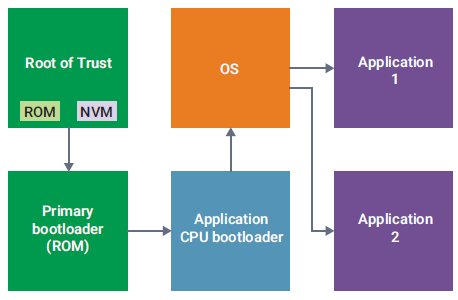
Figure 5: Root-of-Trust Needs Non-Volatile Memory (NVM)
The secure boot starts with instantly verified and authenticated firmware. Both the firmware and the encryption keys for authenticating the firmware are stored in the secure Root of Trust module within the SoC. The firmware is typically stored in a Read Only Memory (ROM), and the secure keys that authenticate the firmware are stored in a separate NVM.
The ROM code is decrypted using the secure keys stored in the NVM within the Root of Trust, thereby making the code secure and trusted. The code executed by the primary bootloader is considered secure and trusted as well since the contents of the Root of Trust module are executed here. The primary bootloader executes the code for the application CPU bootloader, which is also considered secure and trusted. Subsequent code executions by the application CPU bootloader, the operation system, and applications running on the device thus run inherently secure and trusted code.
The entire secure boot flow is nothing but building a “chain of trust.” The Root of Trust is crucial to ensuring a secure and trusted boot flow. Since so much depends on the proper authentication of the code stored in the Root of Trust, the keys should have persistency when the device is powered off, meaning that they must be stored in an NVM.
NVM Requirements for Secure Root-of-Trust
Keys stored in the NVM in the Root of Trust need to be unalterable, so after the product maker has programmed the keys once, they should not be re-programmable. One-Time-Programmable (OTP) NVM is therefore the only choice for implementing a secure Root of Trust.
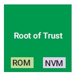
Figure 6: OTP is the only choice for implementing a secure Root-of-Trust
Since OTP memories can be implemented in a few ways, choosing an OTP based on inherently secure technology is imperative to resisting and thwarting attempts by hackers to gain undue access. The OTP must be reliable, area efficient, and consume less power as smart connected home devices come in various form factors, are cost sensitive, and sometimes battery operated. Access time of the OTP is also important to accelerate the boot time of the entire system.
Not all OTP NVM is Equally Secure
Embedded OTP NVM can be based on floating-gate, Electric-fuse (e-fuse), or antifuse technology, each of which has implications for security.
Floating-gate OTP NVM traps charge on a floating gate to store a binary digit and deplete the charge to erase it. Trapping and depleting charge requires high supply voltages, while creating a floating gate and its associated insulating oxide means adding manufacturing steps to a standard CMOS process. The data in a floating-gate OTP NVM can be erased by exposure to ultraviolet light or radiation, giving hackers an opportunity to manipulate its value.
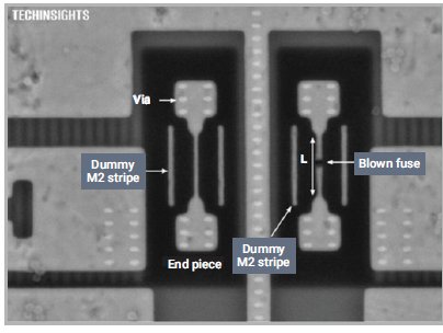
Figure 7: Enlarged view of a programmed TSMC 20nm electrical fuse in a HKMG process Source: Techinsights
E-fuse based OTP NVM replaced floating-gate OTPs in advanced process nodes because floating-gate OTP NVM typically does not scale well below 40nm, so semiconductor foundries provide them to customers as process enabling IP. Programming e-fuses involves breaking continuously etched polysilicon or metal lines to create an open circuit, which is achieved by exploiting electromigration. However, e-fuses are the least secure because inspection under a scanning electron microscope (SEM) easily reveals which fuses have been programmed vs. those that are not, lending themselves to be reverse engineered by hackers.
Antifuse OTP NVM—Inherently Secure
Antifuse OTP NVM is created on the principle of oxide breakdown. Every CMOS device uses oxide as an insulator between the gate and the channel. High voltage applied to the gate of a CMOS transistor causes the oxide breakdown and programs the OTP. Other transistors that do not have high voltage applied to their gates remain unprogrammed. Since no charge is stored or trapped, the OTP NVM is not susceptible to hacking techniques based on altering the device’s supply voltage or temperature. Oxides in modern standard CMOS process technologies are very thin and of the order of tens of Angstroms (each Angstrom is a 10th of a nanometer), making the broken oxide invisible to electron microscopy, so the NVM cell’s state cannot be read out. With these advantages, it is clear why antifuse-based OTP NVM has become the de facto solution for storing encryption keys securely in hardware.
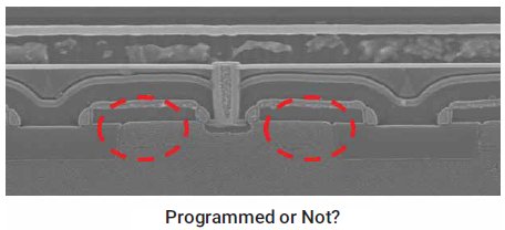
Figure 8: Antifuse-based OTP is inherently secure—it’s impossible to tell if this OTP has been programmed
Security-Enhanced OTP NVM
Even though antifuse OTP is fundamentally physically secure, steps can be taken in the design of the OTP to further enhance it.
High voltages applied to the OTP NVM on unprogrammed locations can program the memory and alter the initial content. To prevent accidental or purposeful programming with high voltages, the OTP must be designed to detect tampering events that include applied voltages that are out of the specified operating range of the SoC. The OTP NVM should raise a flag when such events are detected so that the security engine within the SoC can take appropriate action to disable the attempt or lock access to the OTP NVM.
In addition to tampering, if hackers attempt to access data, the OTP NVM should detect it and send a signal to the embedded processor to take evasive action. Data tampering should be met with preventative action with incorrect data being sent to the output bus of the OTP NVM to befuddle the hacking attempt. Hackers often use a technique called differential power analysis (DPA) to reverse-engineer the contents of OTP NVM. DPA relies on reading the power signature emanating from programmed vs. unprogrammed locations and finding the pattern of the stored content. OTP NVM designed to protect against DPA attacks need to be data agnostic in their programming, meaning that regardless of the content stored in the OTP NVM, the power signature should be the same and should be uniform. Security-oriented OTP NVM architectures include other features like data obfuscation, which generates continuous stream of data on the output bus between read cycles, security locks to disable bits or sections of OTP NVM, and disabling programming an address after it has been programmed once.
Synopsys OTP NVM Based on Inherently Secure Antifuse Technology
Synopsys DesignWare OTP NVM IP is based on the inherently secure antifuse technology. Synopsys is the technology and market leader in antifuse-based OTP NVM with products in volume production for 180nm to 10nm process technologies. Synopsys OTP NVM IP is built on two different OTP NVM bit cells, both of which are patented and have proved to be area efficient, scalable, and reliable in multiple process technologies and foundries. The antifuse-based OTP NVM is fundamentally secure not only because programmed bits can’t be distinguished from unprogrammed bits, but also because there is no charge to erase as in a floating-gate structure. Since the programmed state of a bit within an OTP memory array is independent of charge, there is no leakage in the programmed state and attempts to reverse-engineer information stored in the OTP will likely be unsuccessful.
Taking Security Further with Synopsys DesignWare XSC OTP NVM
Synopsys DesignWare XSC OTP NVM incorporates additional security logic in the periphery of the OTP NVM to resist, detect, and stop hacking attempts. These design enhancements make the OTP NVM an ideal choice for semiconductor companies that need to build a tamper-resistant IOT product. The XSC OTP NVM is available in bit counts up to 32Kb to help secure essential program code and data and encryption keys in connected home devices.
Conclusion
The market for piracy is huge and hackers have become increasingly sophisticated even when security is implemented in hardware. The race between the aggressors and protectors is a battle without end. Smart connected home devices are increasingly storing and processing very sensitive and private user data in addition to attempting to deliver copyright protected content from service providers. Protecting consumer data is vital. The semiconductor industry has converged on the idea of Root of Trust to secure and authenticate home IOT devices. Secure antifuse-based OTP NVM is central to implementing the Root of Trust. Embellishing the OTP NVM with advanced security features further protects the valuable assets of the smart home device maker and consumers. The reputation of companies providing home IOT devices and services is on the line. Today, security drives product design decisions. OTP NVM based on antifuse technology and enhanced with security features delivers on the promise of attack resistance and has become the choice of this market segment and many others including applications targeting the mobile, military-aerospace, and automotive markets.
Related Semiconductor IP
- NVM OTP in Huali (40nm, 28nm)
- NVM OTP in Tower (180nm, 110nm)
- NVM OTP in GF (180nm, 130nm, 65nm, 55nm, 40nm, 28nm, 22nm, 12nm)
- NVM OTP in UMC (180nm, 153nm, 110nm, 90nm, 80nm, 55nm, 40nm, 28nm, 22nm)
- NVM OTP in TSMC (180nm, 152nm, 130nm, 110nm, 90nm, 65nm, 55nm, 40nm, 28nm, 22nm, 16nm, 12nm, N7, N6, N5, N4P)
Related White Papers
- Securing a 4G-connected Smart Meter Gateway with CHERI
- Let's make RISC-V connected systems synonymous with security
- Calibrate and Configure your Power Management IC with NVM IP
- Ensure Cybersecurity in the Connected Vehicles Era With ISO/SAE 21434
Latest White Papers
- Boosting RISC-V SoC performance for AI and ML applications
- e-GPU: An Open-Source and Configurable RISC-V Graphic Processing Unit for TinyAI Applications
- How to design secure SoCs, Part II: Key Management
- Seven Key Advantages of Implementing eFPGA with Soft IP vs. Hard IP
- Hardware vs. Software Implementation of Warp-Level Features in Vortex RISC-V GPU