An Integrated, Tunable RF Filter: an Enabler for Reconfigurable Front-Ends
Jim Wight, Chief Scientist
Seste Dell'Aera, VP Marketing & Sales
Kaben Wireless Silicon
Abstract
This paper presents the design and performance of a key RF circuit necessary for the realization of a reconfigurable, integrated RF front-end: a tunable frequency, selectable bandwidth, on-chip, “SAW replacement” filter. The on-die tunable filter presented here has a tunable center frequency up to 1 GHz, a selectable bandwidth up to 40 MHz, and an adjacent channel rejection down to 60 dB.
Introduction
Reconfigurable radios promise to provide one transceiver capable of handling multiple wireless Standards, ranging from FM tuners or Bluetooth, to GSM and WiMAX. Although most of the functionality of modulation / demodulation, synchronization, channel equalization, etc. can be performed in the digital (or software) back-end, certain functions such as up / down-conversion, amplification and channel filtering must be performed in an RF front-end. With at least a minimal RF front-end being required, performance for each of the Standards to be supported can be enhanced by designing-in appropriate reconfigurability.
For example, analog filtering in a receiver can minimize the dynamic range and bandwidth required by the A/D's. If this filter can be achieved on-die, at an appropriate, selectable IF frequency, then the classical, robust, super-heterodyne architecture can be reintroduced. This would eliminate the difficulties with IP2, DC offsets, and 1/f noise of a zero IF architecture. Further, if this filter's bandwidth and center frequency can be made adjustable (to accommodate each Standard being supported), then not only will the noise and interference be minimized, it will also enable good frequency planning to avoid inter-modulation products in the super-heterodyne.
An On-Chip Reconfigurable RF Filter
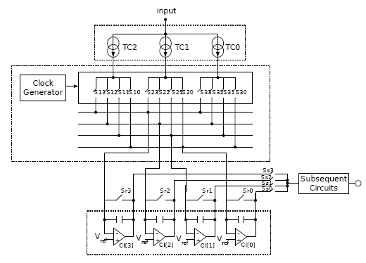
A simplified example of the new, on-chip, reconfigurable RF filter is shown in Figure 1. This filter is comprised of four major elements: a current replicator, that generates multiple tap currents, each proportional to an input signal through constants TC0, TC1, and TC2; a “current rotator”, that sends the tap currents to multiple integrators; multiple integrators, where the number of integrators is one more than the number of tap currents; and an output sampling and resetting circuit.

Figure 1: Sampling RF Filter
The tap current coefficients chosen determine the filter response, HFIR(z) that is achieved:

Here: z = ej2nTi ; k = 1, 2, ... Nt−1 and TCk are the tap coefficients.
The current rotator that is connected to the tap currents, consists of a switch matrix, which is an array of switches coupled between any of the tap currents and any of the following integrators. Each of the integrators, CI[0], CI[1], CI[2], and CI[3] consists of an operational amplifier and a capacitor. Finally, the output sampling and resetting circuit, which selects the correct integrator output at the correct sampling time, consists of output select switches, Ss1, Ss2, Ss3, etc.
Each of the integrators in the sampling RF filter periodically goes through two operating phases; an integrating phase, during which there is at least one current being received, and a rest phase, when no tap current is received. During the rest phase, the integrator's charge is sampled by observing the voltage at its output. This is done by closing the corresponding output sampling switch, connecting the integrator to the subsequent circuits. The voltage on the integrating circuit output is then reset using its reset switch.
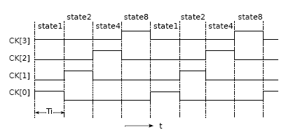
Figure 2 shows the timing diagram for the state changes of the 4 clock buses used in the current rotator of the filter shown in Figure 1. Here, for example, when CK[0] is high, the current from TC0 is integrated onto CI[0], then during the time when CK[1] is high, TC1 is integrated onto CI[0], etc.

Figure 2: Timing Diagram for the Current Rotator Clock Buses
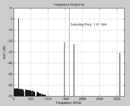
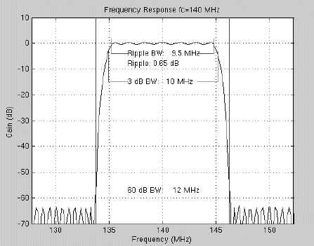
The performance of a 140 MHz center frequency, bandpass filter having 256 tap currents, is shown in Figure 3 (over a wide frequency range), and in Figure 4 (around the pass band). As expected for a sampling filter, undesired pass bands exist on both sides of the sampling frequency. Since the sampling frequency being use by the filter is high (1.61 GHz), these unwanted pass bands are far from the desired pass band. Furthermore, these unwanted pass bands are attenuated by the inherent sinc function operation of the integrating sampler.

Figure 3: Spectral Response of a Band Pass Filter having 256 Tap Currents
As can be seen in Figure 4, a 3 dB bandwidth of 10 MHz is achieved, with excellent pass band ripple (less than +/- 0.5 dB), and excellent adjacent band attenuation (greater than 64 dB).

Figure 4: Pass Band Performance of the Band Pass Filter
Summary
This paper presents the architecture and measured performance for a new Sampling RF filter technology. This filter is a key RF component needed to realize a reconfigurable, integrated RF front-end, able to support multiple Standards.
Related Semiconductor IP
- Wi-Fi 7(be) RF Transceiver IP in TSMC 22nm
- mmWave 8x8 MIMO RF Front End V2
- Low Jitter RF PLL for Sub-1G RF IP Application - SMIC 55nm
- Wi-Fi 6 (ax)+BLEv5.4+15.4 Dual Band RF IP for High-End Applications.
- Wi-Fi 802.11 ax/Wi-Fi 6 /Bluetooth LE v5.4/15.4-2.4GHz RF Transceiver IP for IOT Application in TSMC22 ULL
Related White Papers
- RF front-ends for GSM mobile handsets continue down path of integration
- Reconfiguring Design -> Reconfigurable computing aims at signal processing
- Reconfigurable signal processing key in base station design
- High-Performance DSPs -> Reconfigurable coprocessors create flexibility in DSP apps
Latest White Papers
- Transition Fixes in 3nm Multi-Voltage SoC Design
- CXL Topology-Aware and Expander-Driven Prefetching: Unlocking SSD Performance
- Breaking the Memory Bandwidth Boundary. GDDR7 IP Design Challenges & Solutions
- Automating NoC Design to Tackle Rising SoC Complexity
- Memory Prefetching Evaluation of Scientific Applications on a Modern HPC Arm-Based Processor