Novel and efficient power grid design for lesser metal layer process SOC's
Abstract:
Today semiconductor industry are more emphasizing on the die size reduction and less metal layers technology process options to improve gross margins but as we are decreasing more and more die size, design needs to be closed at higher utilization. Closing the highly utilized design with lesser metal layers option will end up in routing congestion, higher cross talk noise, worsen IR drop. In this paper we propose the novel non-orthogonal metal layer concept in power distribution network for SOC’s which will be able to:
- Increase Routing resources in Design.
- Increase the robustness of power grid network.
- Reduce crosstalk noise.
- Improve IR drop.
Introduction:
In every SOC, Metal layers are distributed in power and signal routes. Metal densities are computed such that the power grid would support aggregate power and IR drop constraints. Power grid refers to the conducting paths which connect power supply to each component. Design of power grid must be such that it should be able to provide power within an acceptable strength to avoid problems such as failure of components, reduction in speed of operation.
Before going in details, let’s discuss some basic concepts like Power Grid structure, crosstalk noise.
Power Grid:
Power grid is the network build with metal layers that is used to supply power to the whole SOC design. For any SOC power grid should be strong enough to have worst voltage drop across the chip within the specifications of the design. Based on the technology options (6M1T/4M1T/7M2T), there are one or two upper metal layers that have low resistivity. The uppermost layer (aluminum layer (AP)) has the least resistance and is mostly used for power-grid design only.
Majority of Designs opt for a conventional mesh type power grid design (orthogonal design) i.e. every layer is perpendicular to its preceding layer and the direction of the each layer is either horizontal or vertical as per the default direction in the technology (shown in Figure 1).
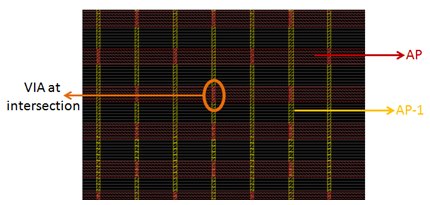
Figure 1: Conventional Mesh type power Grid network
The designer has to work out optimum specifications for the metal layers to be used for the power grid for supporting the IR-drop limits and signal-routing resources in the design. The floorplanner has to avoid the lower metal layers for power because they have high resistance numbers. Also, being thin layers, these lower layers are generally used for signal resources.
4M1T states that design has 4 thin metal layers and 1 thick metal layer. Similarly for 6M1T there are 6 thin metal layers and 1 thick metal. The thickest metal is AP is generally used for power.
Cross talk noise:
CROSSTALK noise is defined as the change in the voltage waveform of a net in an undesired way, due to the signal activity in its neighboring nets, which produce coupling capacitance on it. Crosstalk noise has become a critical design challenge for large, high-performance designs. In noise analysis, the nets on which crosstalk noise is injected by one or more of its neighbors are called the victim nets, whereas the nets that inject this noise are called the aggressor nets. Crosstalk noise can manifest itself in two ways. Functional noise refers to noise that occurs on a victim net which is being held quiet by a driver. Crosstalk noise on such a victim causes a glitch which may propagate to a dynamic node or a latch, changing the circuit state and causing a functional failure. On the other hand, delay noise refers to noise that occurs when two capacitive coupled nets switch simultaneously. Depending on the direction of these transitions, the delays on both nets are affected, giving rise to potential setup or hold time failures.
Problem Description:
Power grid design is a very big challenge to meet SOC power specifications in low metal process (such as 4M1T designs), coupled with the fact:
- Having on chip ballast (where we have only one power source)
- High standard cell Utilization
Conventional mesh type grid is not the efficient for low metal layer process options. Conventional design of grid is based on the concept that every layer need to be perpendicular to its upper and lower layer. Due to this structure, number of vias gets restricted only at the cross section of two adjacent metal layers (as shown in figure 1). Meeting IR drop with conventional grid will also eat up more metal resources. Not only this, other challenges, related to lower metal process are:
- Routing congestion
- Power grid robustness
- Cross talk effect
- Utilization limit
So, keeping all these things in mind, this paper discusses the novel power grid design which is specifically suited for such lower metal process design and can be used for other technology nodes also since this will help in achieving higher std cell utilization by making it routing friendly.
Proposed solution:
AP (the aluminum) is the top most layer (thickest), has the minimum “R” value, so it is dedicatedly used in Power routes (power grid) and Analog routes. Since it is only for power routing, it can be used in any direction i.e. horizontal or vertical (or both) irrespective of the default direction/orientation mentioned in the technology at the designer’s whims for IR drop requirement. Proposed approach implement non-orthogonal metal layer usage for AP layer only, rest all layers retain in default direction as mentioned in technology to design power grid because they are shared in power as well as signals signal. This concept provides the solution for better IR Drop closure, routing congestion and enables to close the design using lesser metal resources in lower metal technology process. Key features in our strategy:
- Better IR Drop
- Enhanced Robustness in power grid network
- Reduction in cross-talk noise
We will discuss this later under comparison and results section.
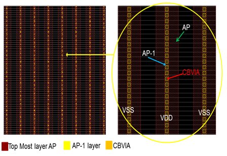
Figure 2: Proposed power grid with non orthogonal implementation
For better understanding let’s take a case study, (4m1t), proposed grid use the top most layer (AP) in the same direction as its lower layer M4 (AP-1), connecting both layers through non-orthogonal VIA (shown in figure 2). AP stripe for power grid is shown in red, AP-1 (M4) is shown in yellow and CBVIA that is connection AP and AP-1 is shown in orange. Using AP in the non preferred direction helps in increase the via count and have significantly improvement in IR Drop. The number of power-stacked via gets much increased because both the stripes for power/ground in AP and AP-1 are overlapping each other and results in robustness of power grid.
Proposed design of power grid also help in reducing cross talk noise, As AP is used in same direction as AP-1. Signal nets (In AP-1) going below AP got the inherent shield (shown in figure 3).
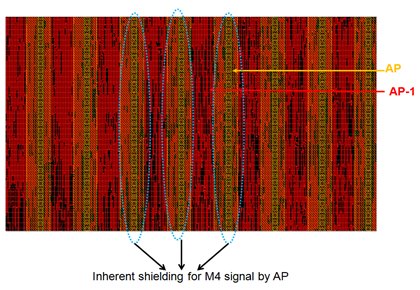
Figure3: Inherent shielding of M4 by AP
For every design, AP resource is used to its maximum utilization level for power grid. Let’s say in x technology, designer is allowed to have maximum density of AP for a chip is 60%. So using proposed approach approximately 60% of the signal routes in M4 (AP-1) automatically gets shields form AP. Designer can plan the routing of critical nets under the shield area.
Comparisons and Results:
IR Drop Improvement
By adopting the two upper most metal layers in same direction and having non orthogonal VIA to connect both metal layers, number of power vias gets increased, IR drop for a chip gets far better. Figure 4 shows the IR drop plots results with conventional power grid as well as proposed power grid with a single power source to make this a worst case for a design.
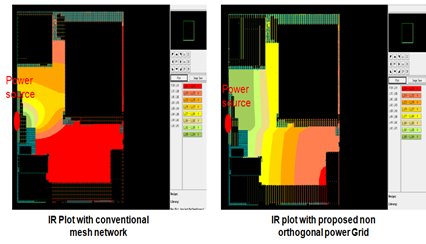
Figure 4: IR drop comparison
Figure 5 depicts the VDD and VSS IR drop numbers with the conventional and proposed grid. With Proposed power grid, IR drops numbers are much improved, with same metal resource utilization in power grids. Proposed design enables 15.7 mV gains in IR drop.

Figure 5: IR drop number comparisons
Robustness of power distribution network:
As in conventional power grid the power via’s only gets inserted at the intersection of the two adjacent metal layers as shown in figure 6. Due to which the count for every 200 micron is restricted to 20 for VDD+VSS.
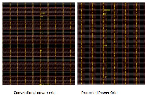
Figure 6: Conventional and proposed power grid
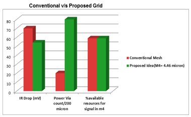
But with proposed grid design Power Via gets inserted throughout the power/ground stripe which makes the count very large. So for every 200 microns with proposed we were able to achieve 400% more power via count without any design overhead. This number is more for lower technology nodes where VIA size is much smaller. Figure 7 shows the comparison.

Figure7: Comparison table for VIA count
Signal Routing Resources Gain Analysis
If we want to achieve the same IR drop with conventional mesh type grid then we will have to increase the width of M4 stripes in power grid. As shown in below table we need to increase the width from 4.46um to 12 um to meet IR drop with convention grid for a case study. We can’t change AP since it is already used maximum as per max density DRC rule.
So by doing this, we eat up signal resources thus increasing the complexity in routing. This will in turn lead to lower SoG utilization. But with proposed grid, we are able to free up routing tracks and hence, achieve higher SoG utilization thus indirectly saving on die size.

Figure 8: Grid specs to meet IR in both cases
Doing a simple calculation for number of signal routing tracks gained with proposed architecture,
Let’s assume metal 4 signal pitch = 0.84um
Testcase design X axis = 3200 um
Total power stripes of metal 4 in design = 3200 / 40.32 (pitch of M4 from below table) = 79
For one power stripe we save 7.54 micron by reducing width of metal 4 from 12 um to 4.46 um
1 micron of metal 4 has 1.19 routing tracks
So for every M4 power stripe we save = 7.54 x 1.19 =8.97 vertical tracks
Total routing tracks saved in case study = 79 x 8.97 = 708 vertical tracks
Total M4 vertical tracks in case study = 3200 x 1.19 = 3808 tracks
%age tracks saved with new power grid = 18.6%
Summary:
Summarizing the complete paper, below graph shows the advantages of proposed grid over conventional power grid having with metal utilizations.
- Able to achieve lesser IR
- Increased power via count
Conclusion
For low metal layers process, due to crunch in routing resources, the design utilization is kept very low to meet the power and routing requirement. With the scheme proposed in this paper, optimal use of resources is done to reduce die-size and still close design with quality and less effort. Hence, smart design technique.
Author’s Biographies:
Gurinder Singh Baghria is a Design Engineer at Freescale Semiconductor, India Pvt Ltd. He is mainly responsible for SoC Physical design activities. Floorplanning, power planning/estimation and IR drop analysis (Static/Dynamic) are his main expertise and focus areas.
Sonal Ahuja is a Senior Design Engineer at Freescale Semiconductor, India Pvt Ltd. She is mainly responsible for SoC backend flow physical Integration activities. Floorplanning, power planning/estimation, padring integration and IR drop analysis (Static/Dynamic) are her main expertise and focus areas.
Azeem Hasan: Working at Freescale Semiconductors, India as Senior Design Engineer and 4 years of experience in Physical Design, Analog Layout Design and Standard Cell Library Design.
Shilpa Gupta: Working at Freescale Semiconductor,India Pvt Ltd. She is mainly responsible for Backend Activities for SoC’s
Related Semiconductor IP
- UFS 5.0 Host Controller IP
- PDM Receiver/PDM-to-PCM Converter
- Voltage and Temperature Sensor with integrated ADC - GlobalFoundries® 22FDX®
- 8MHz / 40MHz Pierce Oscillator - X-FAB XT018-0.18µm
- UCIe RX Interface
Related Articles
- Low Power Design in SoC Using Arm IP
- Multi Voltage SoC Power Design Technique
- BCD Technology: A Unified Approach to Analog, Digital, and Power Design
- The pivotal role power management IP plays in chip design
Latest Articles
- An FPGA-Based SoC Architecture with a RISC-V Controller for Energy-Efficient Temporal-Coding Spiking Neural Networks
- Enabling RISC-V Vector Code Generation in MLIR through Custom xDSL Lowerings
- A Scalable Open-Source QEC System with Sub-Microsecond Decoding-Feedback Latency
- SNAP-V: A RISC-V SoC with Configurable Neuromorphic Acceleration for Small-Scale Spiking Neural Networks
- An FPGA Implementation of Displacement Vector Search for Intra Pattern Copy in JPEG XS