On-chip di/dt Detector IP for Power Supply
Abstract ¡ª This paper demonstrates an on-chip di/dt detector IP. The di/dt detector core consists of a power supply line, an underlying spiral inductor and an amplifier. The mutual inductor induces a di/dt proportional voltage, and the amplifier amplifies and outputs the value. The measurement results show that the di/dt detector output and the voltage difference between a resistor have good agreement.
1 Introduction
As the process technology advances, the number of the transistors on an LSI chip has been increasing and their high speed operations generate more power supply noise while the low supply voltage reduces the noise margin. Thus, the power supply noise becomes a serious issue for the reliability of the LSI operations.
Recently, a di/dt noise is becoming one of the dominant source of the power supply noise along with an IR drop. An EMI noise also becomes a serious problem for high speed operating LSIs. Therefore, a current measurement technique, especially a high frequency di/dt measurement technique, is necessary in order to estimate the di/dt noise.
Many techniques have been proposed to measure the power supply voltage bounce[1]. On the other hand, only few techniques have been developed for the power supply current measurement. One technique uses a resistor connected in series to a power supply line on a PCB board and measures the voltage difference of the both terminals using electron-beam probing[2]. This technique needs numerical calculation to obtain the current and di/dt waveforms. Another technique picks up the magnetic field and measure the spectrum[3]. It is unable to reproduce the original current nor di/dt waveforms from the spectrum because the phase information is lost.
This paper demonstrates an on-chip di/dt detector

Figure 1: Block diagram of the di/dt detector circuit. The bold lines represent outside devices.
IP[4]. This IP can be applicable for feedback substrate noise cancelling[5], feedback di/dt noise control[6] and so on because the detector is realized on-chip and outputs the di/dt value in real time.
2 Circuit Design
2.1 Basic Concept
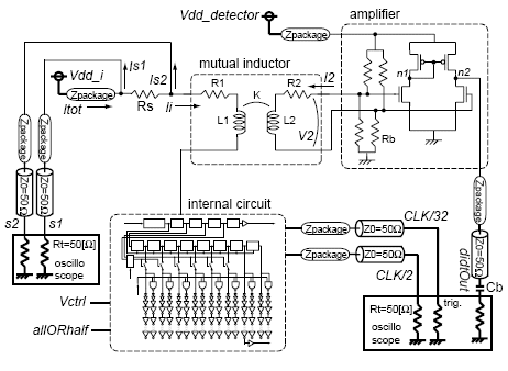
Figure 1 shows the block diagram of the di/dt detector circuit. A power supply current for the internal circuit goes through the power supply line inductance L1. A pickup inductance L2 coupled to L1 with a coupling coefficient K induces a di/dt proportional voltage. A noise-tolerant amplifier amplifies the induced voltage and outputs to a 50¦¸ transmission line that enables a high frequency measurement. The detailed circuit with the measurement setup is shown in Fig.2.
2.2 Mutual Inductor
The inductance L1 should be small since it is in series connection to the power supply line. The small inductance requires a high coupling coefficient K and a bigger L2 in order to generate the enough induced voltage on the terminal of L2. The mutual inductor consists of the power supply line and an underlying spiral inductor. The power supply line has straight layout with v Figure 2: Over-all circuit with the measurement setup.

Figure 2: Over-all circuit with the measurement setup.
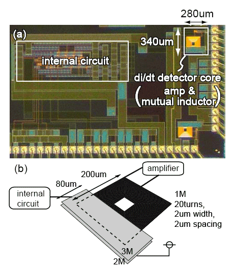
80¦Ìm width using ML2 and ML3 together to reduce the parasitic impedance. The spiral inductor has 20 turns with 200¦Ìm diameter, 2¦Ìm width and 2¦Ìm spacing using ML1, as shown in Fig.3. The equivalent circuit is included in Fig.2.
2.3 Amplifier and Output buffer
Since the output di/dt value is a high speed analog signal, a high frequency and high linearity amplification is the key issue for the amplifier design. The amplifier schematic is also shown in Fig.2. We employ a current mirror type amplifier without current source. The resistors Rb are used to keep the DC bias voltage as half-vdd. The resistance is big enough to be considered open for AC signal.
The output is connected to a transmission line whose characteristic impedance is 50¦¸. The blocking capacitor Cb is inserted at the input port of the oscilloscope to prevent the bias point change of the node n2 due to the 50¦¸ termination resistor connected to GND. Note that the average of di/dt value is zero because the current value is finite, so that the blocking capacitor does not affect the measurement.
2.4 Overview and Measurement Setup
As shown in Fig.2, the power supply line has an onchip resistor Rs in series, the both terminals of which are connected to output pins as s1 and s2 in order to enable the current measurement by calculating the voltage difference, and compare the result with the di/dt detector output as a reference.
3 Analytical Model
3.1 Equations
The mutual inductance ![]() . Assuming that the internal current is Ii and the input current of the amplifier is I2, the output voltage of the mutual inductor V2 is
. Assuming that the internal current is Ii and the input current of the amplifier is I2, the output voltage of the mutual inductor V2 is
Here I2 is small enough because the input impedance is large enough compared with R2 and ¦ØL2 (¦Ø << 10GHz).
Assuming that the gain of the amplifier is G, the output voltage VdidtOut of the di/dt detector circuit is
![]()
which means

where
![]()
Integrating eqn(3) with respect to time,

The relation between the internal current Ii and the voltage of s1, s2 is
![]()
and this equation can be converted to

using Is = Vs/Rt, where Rt is the termination resistance 50¦¸. From eqn(5) and (7),

Differentiate eqn(8) by time,

3.2 Designed Parameters
The equivalent circuit of the mutual inductor is extracted using FastHenry 3D field solver as L1=0.26nH, R1=0.14¦¸, L2=52.3nH, R2=212¦¸ and K=0.25.
According to HSPICE simulations, the gain of the amplifier G is 0.76, the cut-off frequency is 3.3GHz when no load capacitance, and the output linearity range is about ±0.35V.
The series resistor Rs on the power supply line is formed using gate-poly with silicide, and the designed resistance value is about 2.3¦¸. The bias resistor Rb is formed using gate-poly without silicide and the designed value is about 10k¦¸.
4 Measurement Results
4.1 Setup
The chip was designed and fabricated using 0.35¦Ìm 2-Poly 3-ML standard CMOS technology. The chip area is 3.0mm×1.8mm and the chip photograph is shown in Fig.3. The area of the di/dt detector core is 340¦Ìm×280¦Ìm.

Figure 3: (a) Chip photograph. The chip area is 3.0mm×1.8mm. The area of the di/dt detector core is 340¦Ìm×280¦Ìm. (b) Mutual inductor structure.
4.2 Sensitivity of the di/dt detector
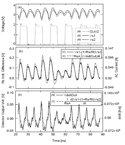
Figure 4 shows the waveforms of (a) CLK/2, s1 and s2, (b) Vs1 − (1 + Rs/Rt)Vs2 signal and the numericaltime- integral of the di/dt detector output multiplied by RsAv2didt, based on eqn(8), (c) the di/dt detector output and the numerical-time-differential of Vs1 − (1 + Rs/Rt)Vs2 signal divided by RsAv2didt, based on eqn(9). Since the Vs1 − (1 + Rs/Rt)Vs2 waveform is noisy, we applied a smoothing before the numerical differentiation. The (M) and (C) in the signal caption represent the measured and calculated waveforms, respectively. The current and di/dt values on the right vertical axis in the graph (b) and (c) are calculated using Rs=2.04¦¸ and Av2didt=1.43×10⁹, respectively.
These graphs show that the currents measured by the series resistor voltage difference and the di/dt detector output have good agreement, and our di/dt detector circuit works well.

Figure 4: Waveforms of (a) CLK/2, s1 and s2, (b) Current waveforms, (c) di/dt waveforms.
4.3 Accuracy of the di/dt detector
The series resistance value Rs can be estimated from s1 and s2 voltage difference. Since the internal circuit does not consume current at the time just before the CLK edge under a low speed operation because of no switching, the DC current going through the series resistor is the same as the current going into the termination resistor Rt of s2, and Is2 = Vs2/Rt. The series resistance value is evaluated by Rs = ¦¤V/Is2 = Rt¦¤V/Vs2 = 2.04¦¸. The designed value Rs=2.3¦¸ is a rough estimation, and the measured value 2.04¦¸ is reasonable.
The error between the solid lines and the dashed lines in Fig.4(b) and (c) are evaluated by the standard deviation,

from 22ns to 72ns region, and the number of the sampling points N is about 750. The error in the graph (b) is ¦Ò=9.10mV which corresponds to 4.46mA, and the error in the graph (c) is ¦Ò=6.30mV which corresponds to 9.01mA/ns.
4.4 Input Impedance of the di/dt detector
The primary part L1 and R1 of the mutual inductor is inserted in series to the power supply line, and the impedance disturbs the power supply voltage for the internal circuit. According to an HSPICE simulation using the parasitic impedance extracted by FastHenry and the current waveform shown in Fig.4(c) dashed line, the voltage drop between the terminal is about 15mV which is acceptable for real applications.
4.5 Constraint
The followings are the constraint of our di/dt detector IP. 1) Frequency response of the amplifier (¦Øcut > ¦Ødidt). 2) Impedance of the secondary spiral and the load capacitance (|R2 + j¦ØdidtL2| < 1/¦ØdidtCload). 3) Resonance frequency of the secondary spiral inductance and the load · parasitic capacitance (¦Ødidt < 1/¡ÌL2C). Here, the load capacitance means the input capacitance of the amplifier. The parasitic capacitance includes the capacitance of the secondary spiral ¡ª the substrate, and the capacitance between the adjacent spiral wires.
5 Conclusion
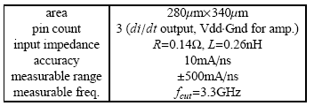
The on-chip di/dt detector IP has been demonstrated. The measurement results show that the di/dt detector output and the voltage difference between a resistor have good agreement with the accuracy of 9.01mA/ns. The characteristics of this IP is summarized in Table1.
Table 1: Characteristics of the di/dt detector IP

Acknowledgement
The VLSI chip in this study has been fabricated in the chip fabrication program of VLSI Design and Education Center(VDEC), the University of Tokyo in collaboration with Rohm Corporation and Toppan Printing Corporation. This study was supported by Grant-in-Aid for JSPS Fellows of the Ministry of Education, Culture, Sports, Science and Technology.
References
[1] Makoto Takamiya, Masayuki Mizuno, Kazuyuki Nakamura, ¡°An on-chip 100GHz-sampling rate 8-channel sampling oscilloscope with embedded sampling clock generator,¡± in Int. Solid-State Circuit Conf. Dig. Tech. Papers, Feb. 2002, pp.182¨C183.
[2] Keith A. Jenkins, Robert L. Franch, ¡°Measurement of VLSI Power Supply Current by Electron-Beam Probing,¡± IEEE J. Solid-State Circuits, vol. 27, pp.948¨C950, June 1992.
[3] H.Wabuka, N. Masuda, N. Tamaki, H. Tohya, T.Watanabe, M. Yamaguchi, K. Arai, ¡°Estimation of the RF current at IC power terminal by magnetic probe with multilayer structure,¡± IEICE Technical Report, EMCJ98-6, pp.39¨C43, May 1998.
[4] Toru Nakura, Makoto Ikeda, Kunihiro Asada, ¡°On-chip di/dt Detector Circuit,¡± IEICE Trans. on Electronics, vol.E88-C, No.5, pp.782-787, May 2005.
[5] Toru Nakura, Makoto Ikeda, Kunihiro Asada, ¡°Feedforward Active Substrate Noise Cancelling Technique using Power Supply di/dt Detector,¡± in JSAP/IEEE Symposium on VLSI Circuits, pp.284¨C287, June 2005.
[6] Toru Nakura, Makoto Ikeda, Kunihiro Asada, ¡°Autonomous di/dt Noise Control Scheme for Margin Aware Operation,¡± in European Solid State Circuit Conference, pp.467¨C470, Sept. 2005.
Related Semiconductor IP
- ReRAM NVM in DB HiTek 130nm BCD
- UFS 5.0 Host Controller IP
- PDM Receiver/PDM-to-PCM Converter
- Voltage and Temperature Sensor with integrated ADC - GlobalFoundries® 22FDX®
- 8MHz / 40MHz Pierce Oscillator - X-FAB XT018-0.18µm
Related Articles
- Power Management for Internet of Things (IoT) System on a Chip (SoC) Development
- The pivotal role power management IP plays in chip design
- One Platform, Five Libraries: Certus Semiconductor’s I/O IP Portfolio for Every Application on TSMC 22nm ULL/ULP Technologies
- FinFET impact on dynamic power
Latest Articles
- An FPGA-Based SoC Architecture with a RISC-V Controller for Energy-Efficient Temporal-Coding Spiking Neural Networks
- Enabling RISC-V Vector Code Generation in MLIR through Custom xDSL Lowerings
- A Scalable Open-Source QEC System with Sub-Microsecond Decoding-Feedback Latency
- SNAP-V: A RISC-V SoC with Configurable Neuromorphic Acceleration for Small-Scale Spiking Neural Networks
- An FPGA Implementation of Displacement Vector Search for Intra Pattern Copy in JPEG XS