OCP-IP Compliance for Databahn Memory Controller Cores
By Nandan Nyampally
Denali Software, Inc.
reprinted with permission by OCP-IP - (C) Copyright 2003 OCP-IP
As SOC applications become a reality for an increasing number of design teams, the focus begins to shift towards architectures and IP that can satisfy the critical and ever-increasing requirements for memory bandwidth. A comprehensive solution to the SOC memory bandwidth problem has two main components. The first is an on-chip communication sub-system that is efficient, non-blocking and flexible. The second is a memory subsystem that provides optimal performance for the application at hand. As time-tomarket windows get progressively smaller, the configurability and completeness of the combined solution becomes increasingly important.
As the leading provider of memory controller cores for off-chip memory, Denali has supported a wide variety of system-level interfaces to its Databahn cores. In particular, our customers using interconnects based on the OCP protocol, such as Sonics' SMART Interconnect IP™, gain a very high-performance infrastructure for the onchip communication sub-system with the following key advantages:
- Split transaction bus for pipelining multiple read requests
- Separate command and data channels to enhance throughput
- Burst oriented transactions for packetized operations and pre-fetching
These features are significant in that they enable our Databahn controllers to utilize separate command and data channels for higher throughput and make intelligent choices by looking ahead at operation requests (utilizing idle cycles for bank manipulations, preparing for other transactions).
Designing a high-performance memory subsystem also requires significant effort due to:
- Complexity of new and emerging high-speed memories such as DDR-SDRAM, FCRAM, RLDRAM, and DDR/QDR-SRAM
- Dataflow and algorithmic requirements to optimize throughput; each memory architecture has its own optimal traffic management solution
- Vendor-specific device implementations of the various memory protocols; each vendor incorporates subtle feature/functionality nuances that must be managed by the controller
- The sophisticated data capture, IO and physical requirements of higher speed operation
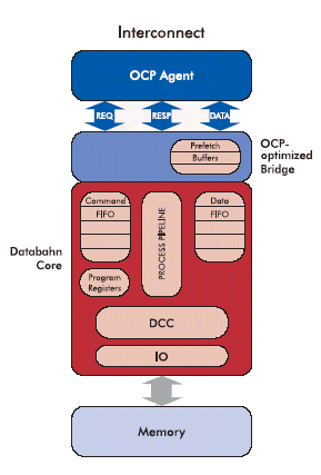
Denali's Databahn product provides a configurable and programmable, OCP-savvy memory controller that is designed to provide optimal performance with each different class of highspeed memory. It is designed with separate command and data channels. Configurable command and data FIFOs control look-ahead and buffering to handle performance-area tradeoffs. Databahn is pipelined to take advantage of lookahead information. This enables it to parallelize control, interrupt transactions, activate and precharge banks and perform other memory maintenance activity.

Databahn also takes advantage of the burst information from the OCP bus to do speculative prefetches. This limits exposure to wasted prefetch transaction by regulating transaction size (this is programmable) and efficiently interrupting transactions. It reduces overhead for speculative writes by delaying commit to the last possible cycle. In process writes that need to be curtailed is masked out.
The combination of the OCP-based SMART Interconnect IP and Databahn memory controllers provide a significant advantage to SOC designers that address key system design requirements: configurability, completeness and performance.
Databahn is currently licensed by 35 semiconductor and system design companies and has been successfully implemented in silicon in 13 different designs, each with different performance and feature configurations. Databahn cores are library independent and cover solutions from .18-micron to .08-micron technologies and DRAM device frequencies from 100-400MHz (200-800MHz data rate).
For further information about Denali, visit www.denali.com.
Related Semiconductor IP
- ReRAM NVM in DB HiTek 130nm BCD
- UFS 5.0 Host Controller IP
- PDM Receiver/PDM-to-PCM Converter
- Voltage and Temperature Sensor with integrated ADC - GlobalFoundries® 22FDX®
- 8MHz / 40MHz Pierce Oscillator - X-FAB XT018-0.18µm
Related Articles
- A Direct Memory Access Controller (DMAC) for Irregular Data Transfers on RISC-V Linux Systems
- Scalable Verification Environment Using OCP Compliant Cores and eRM Compliant eVCs
- Transactional Level Modeling (TLM) of a High-performance OCP Multi-channel SDRAM Memory Controller
- The best of both worlds: Optimizing OCP slave memory behavior
Latest Articles
- An FPGA-Based SoC Architecture with a RISC-V Controller for Energy-Efficient Temporal-Coding Spiking Neural Networks
- Enabling RISC-V Vector Code Generation in MLIR through Custom xDSL Lowerings
- A Scalable Open-Source QEC System with Sub-Microsecond Decoding-Feedback Latency
- SNAP-V: A RISC-V SoC with Configurable Neuromorphic Acceleration for Small-Scale Spiking Neural Networks
- An FPGA Implementation of Displacement Vector Search for Intra Pattern Copy in JPEG XS