Multi-Gigabit SerDes: The Cornerstone of High Speed Serial Interconnects
by Jerry C. Chen -- Genesys Logic America, Inc.
As the CPU speed reaches 3GHz and beyond, the I/O performance of a PC has increasingly become the bottleneck of the overall system performance. Traditionally, the I/O- subsystems are connected to the CPU through the PCI or PCI-X bus. But it is getting more and more difficult to improve the performance with a multi-drop parallel bus such as PCI and PCI-X. For example, the tolerance in timing skew between parallel signals in a multi-drop environment is approaching the practical limit achievable in low-cost FR4 printed circuit boards. In addition, the relatively high voltage levels specified in the legacy parallel buses are incompatible with the reduced supply voltages used in advanced CMOS process technologies.
To circumvent the performance limitation and voltage scaling problem posed by the conventional parallel buses, there is an industry-wide mega-trend to migrate the multi-drop parallel buses to point-to-point serial buses. For example, the vintage IDE bus is being replaced by SATA (Serial ATA) and the parallel SCSI bus by SAS (Serial Attached SCSI). In the case of PCI and PCI-X, a serial replacement called PCI-Express (formerly known as 3GIO or Third Generation I/O) has been adopted by PCI-SIG and is supported by over 280 member companies in the Intel Developer Network for PCI Express Architecture. Figure 1 shows a PCI Express based PC that would appear on the market in 2004.
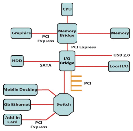
Figure 1. Future PC architecture with PCI Express
In a serial bus, a device called SerDes (Serializer/ Desrializer) is used to transmit and receive data over the serial link as shown in Figure 2. The SerDes can be either a stand-alone device or, in most cases, an IP core integrated into a serial bus controller or an ASIC. In essence, a SerDes is a serial transceiver which converts parallel data into a serial data stream on the transmitter side and converts the serial data back to parallel on the receiver side. The timing skew problem encountered in a parallel bus is solved by embedding the clock signal into the data stream. Since there is no separate clock signal in a serial bus, timing skew between clock and data (which, together with the minimum setup and hold time, determines the maximum data transfer rate) no longer exists. As a result, a serial bus can usually operate at a much higher data rate than a parallel bus in a comparable system environment. For instance, PCI Express specifies a serial data rate of 2.5Gb/s, which translates into a bit period of merely 400ps. But, the tradeoff for the increased data rate is now we have to recover the clock signal from the received serial data stream, which requires more complicated circuitry in the receiver. Furthermore, as shown in Figure 3, the amount of attenuation caused by the lossy FR4 traces on a PC board is significantly more severe at higher frequencies. So, after traveling through some distance on a PCB or through a cable, the received data waveform can be severely distorted. Figure 4 shows the eye diagram of a pseudo-random bit pattern after a 40-in FR4 trace. In addition, reflections caused by impedance mismatch and crosstalks from nearby signals and other impediments can further degrade and corrupt the received signals. Therefore, reliable data transmission over a serial link relies heavily on the robust performance of the SerDes.
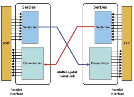
Figure 2. SerDes plays an essential role in serial data communications
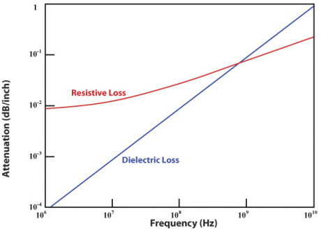
Figure 3. Attenuation caused by the lossy FR4 traces is much more severe at higher frequency
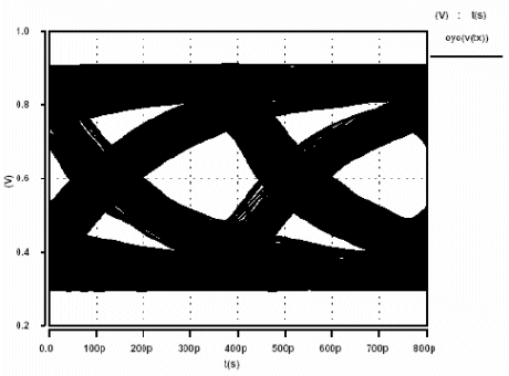
Figure 4. Simulated eye diagram after a 40-inch FR4 trace
Unfortunately, it is not an easy task to design a multi-gigabit SerDes due to the high-speed, mixed-signal circuitry involved and the stringent electrical specifications it has to meet. If the design is started from scratch, it is not unusual for a company to devote a mixed-signal design team for close to a year just to complete the design. It usually takes another year or so and maybe several design spins to make the SerDes mass-production possible. So, either from a cost point of view or a time-to-market point of view, instead of trying to develop the SerDes in-house, for most ASIC designers it makes more sense to license a proven SerDes IP core, unless a discrete SerDes is used which, in most cases, is not cost-effective anyway.
But not all SerDes cores are created equal. Besides cost and performance, there are many other factors to consider. It is important to find a SerDes core that has the right mixture of features needed for the targeted application. In this paper, we review the key issues involved in the design of a multi-gigabit SerDes core and their effects on the performance, power, area and other major attributes of a SerDes. Since more than one SerDes core is needed in most applications, some implementation issues related to the integration of the SerDes core into an ASIC are also covered in this paper. Although PCI Express is used as an example throughout this document, the discussion covered in this paper can also be applied to other high-speed serial buses.
What¡¦s inside a SerDes?
On the surface, the SerDes performs two rather simple functions: serialization and des-serialization. But, to do these two simple functions well at a multi-gigabit speed in a lossy and noisy environment requires a thorough understanding of system-level requirements, a carefully architected clock generation and distribution scheme, some rather complicated mixed-signal circuitry, and full-custom circuit layout (i.e., each polygon is painstakingly drawn by hand). As an example, Figure 5 shows the major functional blocks of a SerDes designed for PCI Express. The parallel input data to the Serializer is usually 10-bit wide since the 8b/10b encoding scheme is used in PCI Express to encode the data. The same 8b/10b code is also used in many other serial buses, such as SATA and SAS, where the serial outputs are AC-coupled. With the 8b/10b code, the transmitted serial data stream is DC balanced (i.e., equal numbers of 1¡¦s and 0¡¦s) to avoid the baseline wander problem commonly seen in an AC-coupled system.
The 8b/10b encoder and decoder are pure digital circuitry and operate only at one tenth of the serial data rate. So, although the 8b/10b encoder and decoder as well as the input and output FIFOs are usually included in stand-alone SerDes devices, for ASICs with integrated SerDes they can be separated from the SerDes and become part of the ASIC¡¦s logic design. For this reason, the encoder, decoder and FIFOs are not included in the discussion of the SerDes core in this paper.
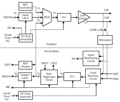
Figure 5. Simplified PCI Express SerDes block diagram
Besides taking the 10-bit parallel data from the AISC, the Serializer can also generate its own parallel test data from the internal BIST (built-in self test) pattern generator. Depending on the design, a variety of BIST patterns can be generated to not only facilitate the debugging and testing of the SerDes design but also to enhance the overall system-level diagnostic capability.
Once the parallel data is latched in, the 10-to-1 multiplexer in the Serializer converts the 10-bit parallel data into a serial data stream. The conversion is done with the clocks generated from the transmit clock generator. A high-speed clock running at the serial data rate is usually required. To reduce cost, this high-speed clock is normally generated from an off-chip low-frequency quartz crystal. As a result, an analog PLL (Phase-Locked Loop) based frequency multiplier in the transmit clock generator is needed. A design challenge for the PLL is to maintain a minimum amount of clock jitter despite all the switching noise generated by the digital logic in the ASIC. For PCI Express, the clock jitter has to be low enough so that the total serial output jitter is less than 120ps. In addition, for the proper operation of the 10-to-1 multiplexer, the PLL generated high-speed clock has to maintain a fixed timing relationship with the 250MHz clock used for latching in the parallel data. With a bit time of 400ps, it is not a trivial task to keep a constant phase relationship between the two clocks over all the temperature, supply voltage and process corners.
The serialized data is driven off-chip and onto the 100£[ differentially terminatedƒn PCB traces by the Serializer using a line driver. To counter the effects of high-frequency roll-off caused by the lossy PCB traces, PCI Express requires the line driver to pre-equalize the output waveform using a technique called ¡§de-emphasis¡¨. When multiple bits of the same polarity are output in succession, all the subsequent bits are driven with amplitude 3.5dB below the first bit. Figure 6 shows a waveform with de-emphasis. By intentionally ¡§de-emphasizing¡¨ the low frequency components of the output waveform, the received waveform will exhibit less ISI (Inter-Symbol Interference) after its high frequency contents are attenuated by the PCB traces.
Similar to SATA and SAS, PCI Express has several power management states that require the line driver to maintain a constant common-mode level with zero differential outputs during Electrical Idle. In addition, the output impedance of the line driver has to be able to switch from low impedance to high impedance and vice versa during these low power states. Furthermore, to detect whether a receiver is present at the far end of the link, PCI Express requires the line driver to have the capability of changing its output common-mode voltage and monitoring the rate that the outputs change to the new value.
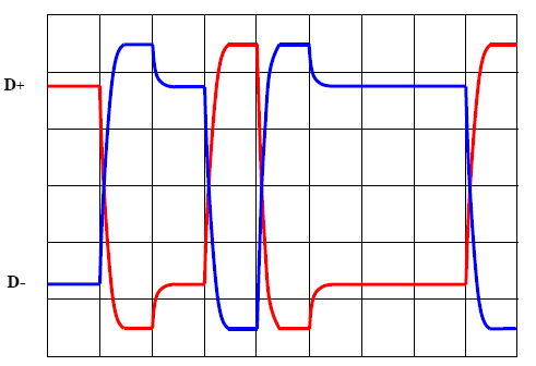
Figure 6. Transmitted waveform with de-emphasis
On the receiver side, there is an input monitoring circuit that monitors the activities on the serial data inputs. During Electrical Idle, the differential voltage on the inputs should be less than 65mV according to PCI Express specifications. When the input differential voltage goes above 175mV, the input monitoring circuit needs to signal the presence of valid data on the inputs. As a result, the De-serializer has to be able to handle an input data stream with a peak-to-peak amplitude as low as 175mV differential.
The received serial data is retimed with the clock recovered from the incoming data stream. PCI Express allows timing jitter (caused by ISI, power supply noise, etc.) up to 60% of the bit time on the input data stream. Therefore, the clock recovery circuit in the De-serializer has to filter out all these timing jitter (i.e., phase noise) and extract a stable clock from it. In addition to timing jitter, the input signals could have a frequency offset up to 600ppm from the local clock. The clock recovery circuit has to have a bandwidth wide enough to track this frequency offset. For systems that implement the Spread Spectrum Clock option specified in PCI Express, the clock recovery circuit also has to track the frequency fluctuation caused by the Spread Spectrum Clock.
Once the serial data is retimed with the recovered clock, it can be converted back to a 10-bit wide data stream with the 1-to-10 de-multiplexer. Similar to the 10-to-1 multiplexer in the Serializer, the operation of the1-to-10 de-multiplexer usually requires a high-speed bit clock that is synchronized with a lower speed byte clock. Since the bit time for PCI Express is only 400ps, the two clocks would have to track each other within as low as 100ps depending on the setup and hold time needed by the latch.
To align the 10-bit parallel data at its 8b/10b encoded byte boundaries, a Byte Alignment Circuit is provided to detect a special alignment character called ¡§comma¡¨ (0011111010 or 1100000101). When the Byte Alignment Circuit is enabled, it looks for the comma characters and aligns the 10-bit outputs with the comma characters. The aligned parallel data is sent to the ASIC along with the recovered byte clock. If the SerDes is in the BIST mode, a BIST pattern checker will check the aligned parallel data against the expected data pattern and flag any bit errors detected.
What makes a SerDes stand out from others?
Some of the challenges in designing a multi-gigabit SerDes have been outlined in the previous section. A good SerDes design has to solve these design problems while keeping power consumption low and footprint small. In this section, we will discuss some of the circuit design techniques that can be employed to tackle these design challenges. We will also discuss some of the features that can make a SerDes design stand out.
Better jitter performance
For a multi-gigabit SerDes, its jitter performance is one of the most important parameters for judging the robustness of the design since the bit error rate is directly affected by the jitter performance. To achieve a BER of 1x10-12, PCI Express specifies a maximum output jitter of 120ps for the Serializer and a minimum input jitter tolerance of 240ps for the De-serializer. For the Serializer, a smaller output jitter means it is less likely that a bit error will occur when the data is received by the De-serializer. In other words, for the same amount of received jitter, we can transmit the data over a longer cable or PCB trace if the Serializer output jitter is smaller
There are many factors that can affect a Serializer¡¦s output jitter but the key is to keep the high-speed clock that is used for clocking out the serial data as jitter-free as possible. The serial clock is typically generated by a PLL-based frequency multiplier from a slower reference clock. Figure 7 shows the major functional blocks of a PLL where the reference clock¡¦s frequency is multiplied by a factor of N/M to generate the output clock
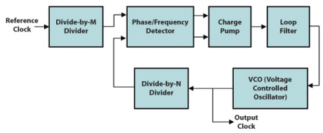
Figure 7. Simplified block diagram of a clock-multiplying PLL
In addition to the PLL, there are other areas where improvements can be made to reduce the serial output jitter. For example, the clocking on the 10-to-1 multiplexer; paying attention to the layout on power and ground; employing an auto-calibration circuit to do the on-chip termination; dealing electrical properties carefully on packaging.
On the receiver side, the De-serializer¡¦s jitter performance is judged by the maximum amount of jitter riding on the incoming data stream it can tolerate. Since the received data is retimed by latching the data with the recovered clock, a bit error can occur only if either the clock or the data is too early or too late. So, in general the De-serializer¡¦s input jitter tolerance can be improved by making the clock less likely to be early or late and/or making the data less likely to be early or late. In other words, we need to reduce the jitter on the recovered clock and/or the received data.
The recovered clock is generated by the clock recovery circuit in the De-serializer. The clock recovery circuit is usually based on a PLL similar to the one shown in Figure 7. So, the techniques discussed before for reducing a PLL¡¦s output clock jitter can also be applied to the clock recovery circuit. But, contrary to a frequency-multiplying PLL, the input to the clock recovery circuit is the incoming serial data instead of a stable reference clock. For PCI Express, the frequency of the clock embedded in the incoming data can deviate from the local clock by 600ppm. As a result, the PLL in the clock recovery circuit must have a loop bandwidth wide enough to track this frequency difference.
The amount of jitter on the received data can potentially be reduced by an on-chip equalizer.
The purpose of the equalizer is to reverse the high-frequency attenuation caused by the PCB traces or cables. For PCI Express, the de-emphasis circuitry in the Serializer has already pre-equalized the data before it is transmitted. Therefore, the need for an equalizer in the De-serializer is diminished. Nonetheless, for systems with longer PCB traces or cables, an equalizer in the De-serializer helps improve its jitter tolerance. Lower power and smaller size In many applications (e.g., 8-lane PCI Express links), multiple SerDes cores have to be integrated into an ASIC. For these applications, it is crucial for the SerDes core to be small in size as well as power efficient. It certainly helps in these regards by using a more advanced process technology. But the savings in power and area from scaling for a mixed-signal design such as the SerDes are typically less than what could be achieved for a pure digital design. For example, since both the output swing and impedance are fixed, power dissipation by the line driver only scales linearly with the supply voltage. Furthermore, it may not be economical to use the most advanced process technology for a given application. Consequently, there is a need to minimize power and size regardless what process technology is used. As shown earlier, the Serializer needs a PLL-based frequency multiplier to generate the high-speed clock. Some of the earlier SerDes cores on the market have a frequency multiplier inside each SerDes. As a result, when multiple SerDes cores are integrated into a single chip, there will be the same number of frequency multipliers as the cores on the chip. In newer designs, both power and area are saved by sharing a single frequency multiplier among several SerDes cores in the same ASIC, as shown in Figure 8. But distributing multi-gigahertz clocks over an extended distance consumes a lot of power. In addition, there are signal integrity concerns when a high-speed clock is routed over an extended distance. Therefore, there is a limit on the number of SerDes cores that can share a frequency multiplier. Percentage-wise, the amount of saving in area begins to level off when more and more SerDes cores are sharing the same frequency multiplier. Figure 9 shows the percentage in area saved as a function of the number of sharing SerDes cores for a PLL that is half the size of a SerDes core. Normally, a compromise is to share a PLL by four SerDes cores as shown in Figure 10.
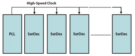
Figure 8. A PLL can be shared by multiple SerDes cores to reduce power and area
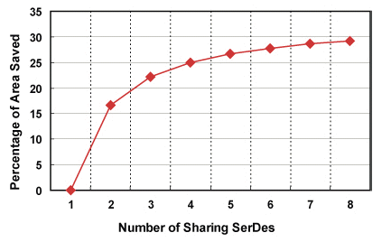
Figure 9. The percentage of area saved begins to saturate when the number of SerDes cores that share a PLL increases.
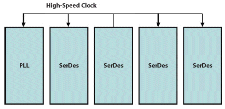
Figure 10. Limiting the number of SerDes cores that share a PLL to four to maintain consistent jitter performance
This PLL-sharing concept can be applied to the De-serializer as well to further reduce power and area. Traditionally, a PLL is used for clock recovery in the De-serializer. However, the PLL in the clock recovery circuit can be replaced by a DLL (Delay Locked Loop) if a high-speed serial clock is available. As shown in Figure 11, a DLL is similar to a PLL with the VCO replaced by a VCDL (Voltage Controlled Delay Line). The delay through the VCDL is adjusted so that the recovered clock is phase-locked to the incoming serial data. The DLL is easier to design than a PLL since it is unconditionally stable. A smaller loop filter can be used in a DLL since its size will only affect the loop¡¦s input tracking capability but not the stability. Furthermore, the VCDL can be implemented as a simple phase-interpolator which is very compact in size. As a result, both power and area of the De-serializer can be reduced by using a DLL in the clock recovery circuit. Since the required high-speed serial clock is available from the shared PLL, both the Serializers and De-serializers can now share a single PLL.
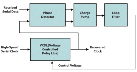
Figure 11. Simplified block diagram of a DLL-based clock recovery circuit
Easier to test
How to test a multi-gigabit SerDes in a volume production environment presents a serious challenge to the ASIC designers. With a maximum frequency usually less than 200MHz, the existing ATE testers simply don¡¦t have the bandwidth to test a multi-gigabit SerDes at speed. On the other hand, dedicated test instruments are either not readily available or too expensive and time consuming for production testing. Consequently, relying on the built-in self test (BIST) functions in the SerDes is the only viable solution.
Most SerDes cores offer BIST functions in the form of a PRBS (Pseudo Random Bit Sequence) pattern generator in the Serializer and a corresponding pattern checker in the De-serializer. In the BIST mode, instead of the normal data inputs, the Serializer takes the parallel data from the BIST pattern generator to generate the serial outputs. The PRBS pattern checker in the De-serializer checks the received data against the expected pattern to determine if there is any bit error. A SerDes can test itself by looping back the PRBS pattern from the Serializer to the De-serializer.
To emulate the worst-case received waveform, typically the PRBS pattern is looped back off-chip through a jitter injection filter, which intentionally injects timing jitter into the data stream. But, constructing a jitter injection filter with the desirable characteristic is not always an easy task, especially for ASIC designers who are not familiar with signal filtering and conditioning at multi-gigabit data rates. A better solution is to include this jitter injection filter in the SerDes core and allow the PRBS pattern to be looped back on-chip through this filter. By doing so, the ASIC designers no longer have to deal with the high-speed signals on the test board. Furthermore, since looping back the serial signals on-chip is only an option, the PRBS patterns can always be looped back externally if necessary.
Besides the PRBS patterns, the BIST function can also include other data patterns that could provide additional diagnostic functions to what a SerDes has to offer. For example, the BIST pattern generator can generate the compliance pattern, defined in the PCI Express specifications, to make system-level diagnosis easier. By generating a constant 1¡¦s or 0¡¦s by the BIST pattern generator, DC level testing on the serial outputs can be easily performed on an ATE tester.
Lower system cost and easier to use
Due to signal integrity concerns, a multi-gigabit SerDes core is normally offered as a hard macro. In order to share the PLL with multiple SerDes cores, careful planning on the circuit layout is required. First of all, the SerDes core¡¦s layout should be implemented in a modular fashion so that any number of SerDes cores can be put together easily for a faster time-to-market. Secondly, since all the high-speed clocks have to come from the PLL, it is necessary to plan ahead on how many SerDes cores a PLL can support and how much buffering is needed. Although it may seem more convenient to buffer the high-speed clocks in cascade (Figure 12), the amount of distortion will accumulate with the passing of each buffering stage and cause the deterioration in jitter performance of the corresponding SerDes core. For more consistent jitter performance, it is better to only buffer the clocks once in the PLL and distribute the clocks directly from the PLL. By limiting the number of SerDes cores supported by a PLL to four as shown in Figure 10, for example, consistent jitter performance can be obtained while making it easy to integrate multiple SerDes cores.
Owing to the 10-bit data bus on the parallel side, most SerDes cores on the market require a reference clock to the PLL with a frequency that is one tenth of the serial data rate. For example, the 2.5Gb/s PCI Express SerDes cores usually require a 250MHz reference clock input. Such a high frequency clock has to be either generated from a separate clock chip or an expensive crystal oscillator. Clearly, neither is desirable from a cost standpoint. A better solution is to design the SerDes core in a way that it can accept a reference clock with a lower frequency. Specifically, PCI Express requires a 100MHz reference clock to be available on both the main board and the adapter board. By designing the SerDes core with a 100MHz reference clock, both the board area and system cost can be reduced.
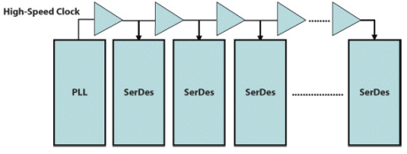
Figure 12. Cascading clock buffers may affect jitter performance
Another cost saving measure is to integrate the termination resistors on-chip. For PCI Express, two 50£[ termination resistors are required for each of the differential serial input and output signals. So, it is a saving of four resistors, both on cost and board space, for each SerDes core. Furthermore, from a signal integrity standpoint, it is necessary to integrate these resistors on-chip so that ringing caused by the package parasitics can be minimized. Although PCI Express has a ±20% tolerance on the resistance value, better matched termination resistors can reduce reflections and improve signal return loss. With the help of an auto-calibration circuit, on-chip resistors can typically keep their value within 5% of the target.
To cover a wide range of applications, it is desirable to have the major parameters of a SerDes core adjustable through the programming of some control registers. For example, the serial output swing can be made programmable so that, when necessary, it can be either increased to reach a longer distance or reduced to save power. Similarly, the amount of output de-emphasis needed is different for different link lengths. By making it programmable the SerDes core can be tailored to meet the specific needs of a given application.
Summary
SerDes plays a crucial role in multi-gigabit serial data communication links. However, due to its high-speed and mixed-signal design nature, it is not an easy task to design a multi-gigabit SerDes that can meet all the stringent performance requirements. In this paper, techniques that can be employed to achieve better jitter performance are discussed. But meeting the electrical specifications for a given application is only the minimum requirement. A good SerDes design also has to be low in power and small in size so that multiple SerDes cores can be easily integrated into an ASIC. In addition, to make low-cost volume production possible, a SerDes core must include all the necessary BIST functions to facilitate production testing. It is also highly desirable to have the features that can reduce the overall system cost and make the system design easier.
About Genesys Logic
Genesys Logic Inc. is a leading provider of advanced I/O solutions for communications and computing equipment. The company¡¦s extensive portfolio of analog and mixed signal solutions and enabling connectivity technologies, including USB, Flash Disk Drive, Ethernet, Gigabit SerDes, IEEE-1394, PCI and PCI Express, provide improved product performance at reduced cost.
Combining its extensive design capabilities, systems knowledge, and valuable intellectual property (IP) into leading products, Genesys Logic counts the world¡¦s leading manufacturers of scanners, printers, cameras, and storage solutions as its customers. Genesys Logic was founded in 1997 and is headquartered in Taipei, Taiwan, with its international operations based in San Jose, California. More information is available at www.genesyslogic.com.
Related Semiconductor IP
- ReRAM NVM in DB HiTek 130nm BCD
- UFS 5.0 Host Controller IP
- PDM Receiver/PDM-to-PCM Converter
- Voltage and Temperature Sensor with integrated ADC - GlobalFoundries® 22FDX®
- 8MHz / 40MHz Pierce Oscillator - X-FAB XT018-0.18µm
Related Articles
- High Speed Serial Interconnects - What to Look for When Selecting an IP Vendor
- Redefining Speed: How FPGAs are shaping the future of high-frequency trading
- Integrating High Speed Serial Transceivers into an FPGA
- Choosing serial interfaces for high speed ADCs in medical apps
Latest Articles
- An FPGA-Based SoC Architecture with a RISC-V Controller for Energy-Efficient Temporal-Coding Spiking Neural Networks
- Enabling RISC-V Vector Code Generation in MLIR through Custom xDSL Lowerings
- A Scalable Open-Source QEC System with Sub-Microsecond Decoding-Feedback Latency
- SNAP-V: A RISC-V SoC with Configurable Neuromorphic Acceleration for Small-Scale Spiking Neural Networks
- An FPGA Implementation of Displacement Vector Search for Intra Pattern Copy in JPEG XS