Moore's Law is Dead: Long Live SoC Designers
As the "Free Lunch" Era Closes, Chip Designers Grow in Value by Providing Innovative Ways to Increase Performance and Cut Power Consumption
By Kurt Shuler, VP of Marketing, Arteris Inc.
Let’s face it, Moore’s Law has been the free lunch program of the semiconductor industry. And now that Moore’s Law is dead, how will SoC designers continue to survive?
In other words, when the free lunch program ends, what is your game plan? How do chip architects continue to provide value to the market when transistors are no longer “free”? Can they overcome the complacency that characterized the Moore’s Law era? I’m betting that that their skills become more important even as transistors become more expensive with each advanced process node.
Many who hope that Moore’s Law will magically get an 11th hour extension will find evidence to the contrary here. It’s clear: transistors get more expensive below 20 nanometer. But that’s okay, when you consider that scalability led to some lazy design practices.
The good news is that performance gains and power consumption reductions will continue for chip designs in the future if SoC designers choose to refactor designs, switch to a more efficient computing architecture and enhance on-chip communications.
Moore’s Law made hardware designers lazy
Up until now, SoC designers could always rely on physics and economics to increase performance, add functionality, reduce power and lower cost for next-generation systems. When performance doubled and power consumption decreased every 18-to-24 months, it didn’t make sense to make efficient IC designs because time to market was everything.
In fact, companies pushed silicon out before all the bugs were worked out. This “Just ship it” attitude usually evolved into a “we’ll fix it in software” mentality. Ultimately, when product performance or power consumption suffered, designers conveniently migrated to the next generation manufacturing process to make chips with smaller, faster and more efficient transistors. A process “shrink” could always overcome a multitude of design “sins.”
The result: The industry became fat and lazy during the free lunch era. People added on to their designs haphazardly and bolted on IP block after IP block to add functionality, without taking the time to globally optimize the entire on-chip system.
Software developers also grew ‘lazy’
Guess what? Software code also suffered bloat during era of Moore’s Law. That’s why the term “Windows Bloat” is a household word. Want proof, read “Windows bloat? It’s always been that way,” by ZDNet’s Ed Bott from 2006, where he outlines the history of Windows up to Vista.
Some want to blame it on a nefarious Wintel plan that drove the constant PC upgrade cycle but in truth, we were all under time to market pressure and we all relied on the next version of faster processors to make the newer version of software bearable.
Eventually, support, maintenance and update problems forced the software industry into the code refactoring process, where software is periodically updated to make it more efficient, maintainable and extensible without changing its external behavior. Improvements in code size, performance and power consumption were the benefits. Interestingly, refactoring will now help the hardware world move beyond the free lunch era.
Moore’s Law really is going to end
Is Moore’s Law really dead?
The short answer is not yet (it’s in triage). But the following data presents the case of why it soon will be.

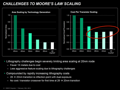
Figure 1. Costs per transistor increase at process nodes smaller than 28 nm (Source: Dr. Lisa Su, AMD and ISSCC 2013)
Dr. Lisa Su from AMD showed that the cost per transistor increases – for the first time in semiconductor history – as the industry advances to smaller process dimension below 28nm. She made this observation during her 2013 ISSCC keynote presentation.
Why? Below 28 nanometers, the wafer costs at newer nodes outweigh the benefit of having more transistors per wafer due to the smaller transistors, according to Dr. Wally Rhines, CEO of Mentor Graphics. He discussed this during his keynote at April’s Electronic Design Process Symposium (EDPS). Costs increase because manufacturers need to perform double or triple patterning to create the smaller transistors. This increase in costs is partly due to the delay in commercially viable next-gen lithography tools. It is also because the process to create FinFETs requires additional masks and process runs.

Figure 2. Costs per wafer increase at process nodes smaller than 28 nm (Source: Dr. Wally Rhines, Mentor Graphics and EDPS 2014)
Andy Grove of Intel and Clayton Christensen of Harvard Business School coined the term “Strategic Inflection Point” in 1998. According to Grove, a strategic inflection point is, “what happens to a business when a major change takes place in its competitive environment.” Reaching the point of diminishing returns for CMOS technology could be the inflection point that unleashes SoC design team creativity and value.
New opportunities for design innovation
The post Moore’s law era presents innovation opportunities that increase the importance of hardware design teams. Here are four areas that present the greatest potential for improvement:
- Hardware refactoring
- Processing efficiency
- Optimizing on-chip communications
- Faster turns
Hardware refactoring
The hardware design teams that examine existing designs to look for performance, power and area improvements within the current process node stand to gain the most. Refactoring existing product architecture RTL will achieve better performance, lower power consumption and less cost without changing functionality.
Part of this process involves standardizing and extending on-chip and off-chip interfaces for the future integration of new IP features. This will help designers reconfigure SoCs quickly in a platform approach to address multiple markets with the same architecture
A big part of this process will be finding and removing the legacy "cruft" or bloat in SoCs. Some of the transistors in your smartphone, for instance, were synthesized from RTL written in the 1990s. Refactoring these older designs will result in better performance and lower power consumption using mainstream semiconductor manufacturing processes.
Asymmetric Multiprocessing (AMP)
Processing efficiency is also an avenue of potential improvement using mainstream semiconductor nodes. Today, general purpose CPUs handle as much processing as possible simply by cranking up the frequency in symmetric multiprocessing architectures. But battery life and power budgets cannot scale as fast as feature growth projections. A change in SoC architecture is required to allow designers to “use the best processing core for the job” and achieve more performance and less power consumption from the same transistors. This will spur a switch to asymmetric multiprocessing architectures (AMP).
There are several advantages to switching to AMP and this concept has been discussed at length, so there’s plenty of arguments for this approach. But now the pressure is greater to switch and the barriers to entry continue to fall.
In 2012, Arteris worked with AMD, ARM, Imagination, MediaTek, Qualcomm, Samsung and Texas Instruments to form the Heterogeneous System Architecture (HSA) Foundation to define interfaces for parallel computation utilizing CPU, GPU, and other devices to support a diverse set of high-level programming languages.
This effort helps AMP architecture adoption by defining standards for hardware and software, thus making it economically viable from a cost perspective. The industry can benefit from additional performance and power savings within familiar transistor technologies.
On-chip communications
The third area for improvement is on-chip communications efficiency. Up to now, SoC architects have focused on computational processing IP and SoC features. But the constraint on overall system performance has shifted to the on-chip fabric as more functionality has been added to a die. Now the emphasis needs to shift to how these IP blocks communicate with one another within the SoC design. How the functionality is connected together will become just as important as the functionality itself.
Reduce interconnect area and power
Increasing chip functionality also consumes more die area at an increasing rate because of the additional transistors and metal line area required for on-chip communications and arbitration. This causes routing congestion and creates timing issues. Since wires don’t scale the same as transistors, they consume greater area and require more metal layers that drive up complexity and cost.
Choosing on-chip communications technology that enables the most efficient connections between IP will enable scalability based on requirements and use cases. Packet-based network-on-chip interconnect technology, for example, can be integrated with power management to allow chips to scale up in size and functionality without blowing out the size of the on-chip fabric, or blowing up the power budget.
Design chips faster
Another way to survive the post Moore’s Law era is to boost productivity in the SoC design stage. For SoCs in the post-Moore’s Law era, the interconnect plays a more important role in this stage.
Whether it’s refactoring existing chips or creating new ones, design teams need to be able to quickly create candidate SoC architectures based on requirements and use cases and simulate those using models. Then they need to review and interpret the simulation data using industry-standard tools, and quickly make changes to the candidate architecture based on that assessment.
Once the architecture is frozen, the interconnect development team needs to be able to quickly make changes to the interconnect fabric to accommodate changing IP requirements late in the design cycle and automatically create the necessary verification test harnesses.
The faster the development team can “turn the crank” with this process, the more they can optimize their design. Choosing an advanced on-chip communications technology allows teams to define, simulate, assess, integrate and verify SoC architectures at a faster rate than ever before.
The on-chip fabric is the logical and physical implementation of a system-on-chip’s architecture, and optimizing the fabric and the communications passing through is required to get the best results from the architecture. If done correctly, design teams can simultaneously reduce SoC power, cost, and design time while increasing debug and tuning efficiency.
It’s all up to SoC design teams
The death of Moore’s Law is actually good for SoC designers because it increases the value of their work. Design teams that choose to refactor existing designs, adopt more efficient processing architectures, and enhance on-chip communications capabilities will emerge successful during this sea change.
Now that free lunch era is over, it’s time to optimize your architecture and eat your competitor’s lunch.
— Kurt Shuler is vice president of marketing at Arteris and has extensive IP, semiconductor, and software marketing experience in the mobile, consumer, and enterprise segments working for Intel, Texas Instruments, and three startups. Prior to his entry into technology, he served in the US Air Force Special Operations Forces.
Related Semiconductor IP
- NPU IP Core for Mobile
- V-by-One® HS plus Tx/Rx IP
- MSP7-32 MACsec IP core for FPGA or ASIC
- 100G / 200G / 400G / 800G / 1.6T MACsec
- 32 bit RISC-V Multicore Processor with 256-bit VLEN and AMM
Related White Papers
- The fixed processor is dead, long live the battery
- Embedded Systems: Programmable Logic -> Embarrassment of riches hinders proper use of Moore's Law
- Embedded Systems: Programmable Logic -> Adaptive tech extends Moore's Law
- Moore's Law, the bifurcation of the semiconductor industry and 3-D integration
Latest White Papers
- Concealable physical unclonable functions using vertical NAND flash memory
- Ramping Up Open-Source RISC-V Cores: Assessing the Energy Efficiency of Superscalar, Out-of-Order Execution
- Transition Fixes in 3nm Multi-Voltage SoC Design
- CXL Topology-Aware and Expander-Driven Prefetching: Unlocking SSD Performance
- Breaking the Memory Bandwidth Boundary. GDDR7 IP Design Challenges & Solutions