Method for Booting ARM Based Multi-Core SoCs
Amitav Halder, Arunendra Tomar, Umesh Pratap, Arun Jain (Freescale Semiconductor India Pvt. Ltd.)
Introduction :
Boot process is the process in which any SoCs takes various device configurations (trim bit, device security settings, boot vector location) and memory initialization (like FLASH/SRAM/GRAM) is done after reset lifting. In the boot process various modules/peripherals (like clock controller or security handing module and other master/slaves) initialized as per the SoC architecture and customer applications. In Multi core SoCs, first primary core (also called booting core) start up in boot process and then secondary cores are enabled by software.
The boot process begins at Power On Reset (POR) where the hardware reset logic forces the ARM core (Cortex M series) to begin execution starting from the on-chip Boot ROM. The Boot ROM code uses the given boot select options as well as the state of various FUSE/straps and GPIO settings to determine the boot flow behavior of the SOC.
What are multi core SoCs:
Multi Core SoCs have more than one processor where each processor has its own specific application.
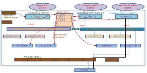
In complex SoC like networking/Automobile application ,Most of the industries SoC integrates primary core (Booting core) ,application/system core , networking cores on a single die to handle various data from different peripherals (Master/Slave) .Primary core is the heart of any SoC that handles the booting and maximum functionality but for heavy traffic data (Ethernet/TDM) and high frequencies(CSI-2,QSPI) applications, we need to have specific application core such as CORTEX-A cores to process the data .
Fig1: Architecture for multicore SoCs
Booting Flow for multi core SoCs:
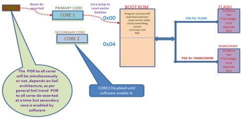
When the device gets POR, the primary core jump to reset vector location. The reset vector is the location is mapped to the ROM start address (also called boot ROM), from where the core will start execution after POR. ARM processors (like Cortex-M series) use a reset vector located either at 0x00000000. The decision is made through a configuration input signal and hence can vary between different SoCs.
Once primary core (like ARM Coretx-M) is out of reset it will start executing from memory address location 0x00000000. The primary core loads the program counter and starts executing from address 0xSP(Primary core stack pointer , inside ROM at 0xSP location it’s stack pointer will be loaded) which instructs the core to load its reset handler (stack pointer, vector table) and read processor Start Address(PSA) to get application boot address and jump to that location.
At the PSA, the hex file or image is loaded by boot loader. This address can be of SRAM/GRAM or FLASH.
CORE will execute the Image/.hex from PSA which is likely to load at SRAM/GRAM or FLASH as directed by Boot Loader.
The loading of Image/.hex into memory (FLASH/SRAM/GRAM) is done by boot loader. This loader can be inbuilt with BOOT ROM or can be external loader.
In SoC verification, the hex file/image is generated from .c file(pattern) by compiler -> assembler -> linker->.ELF->.HEX.
Fig2: Booting sequence of primary core in Multicore SoCs
Primary core already Boot up and ready to remove the rest for RESET for other peripheral as well as secondary core as by default secondary core is disabled which is enabled by software.
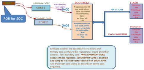
Once software decides to enable the secondary core, the corresponding registers (depends on SoC architecture, which enable secondary core and clock controlling registers) needs to be programmed using the primary core .Once secondary core is enabled, this will start fetching data from the reset vector location (which will be different that was for primary core like reset vector location for primary core is 0x00000000 than for secondary core the reset vector location can be 0x00000004).
Actually Secondary core also boot from 0x00000000 and by using the virtualization concept (Memory mapping from 0x00000000 to 0x00000004) or bus probing concept, it has to map on 0x00000000 address to 0x00000004 and fetch first instruction form this address as well .
Now secondary core loads the program counter and starts executing from address 0xSP(Secondary core stack pointer) which instructs the core to load its reset handler (stack pointer, vector table) and read PSA to get application boot address and jump to that location.
Fig3: Booting sequence of secondary cores in multicore SoCs
Fig4: Multi core enabled
There are separate Image/.hex for primary core and secondary core. The Image/.hex should store different memory locations (i.e.GRAM/SRAM/FLASH) for all core . This indicates that the PSA is different for all the cores. This setup is the part of SoCs architecture and decided by the linker files for all the cores. For example the linker file which tells the Image/.hex files addresses and starting address will be PSA .
For example: Image/hex start and end addresses generated according to linker file.
CORE1-0X3E800000-0X3E80FFFF
CORE2-0X3E810000-0X3E81FFFF
CORE3- …..
What is Boot loader :
Depending on SoC architecture and implementation, boot loader can be a part of boot ROM or outside the boot ROM.Boot loader is program which loads the image/hex into the memory as per Fuse/straps configuration. Boot loader is a program which has the data structure of all the peripheral and booting interfaces. Boot loaders are highly core and board specific. Boot loader will be executed on POR to SoC.
Responsibilities of Bootrom:
- Performs the essential initialization including programming the PLL,clocks, stacks, interrupt set up, watchdog timers etc.
- Enable the different L1 cache .
- Configures I/O elements and pin multiplexing based on the Fuses/Straps pin value.
- Initializes the flash controller to default settings.
- Load user code from flash (NOR, NAND), external memory, SD/MMC, USB or UART. Boot order and options are set by fuses/straps pins.
Features of the ROM include:
- Support for booting from various boot devices
- Serial Downloader support (USB, Flex CAN and UART etc.)
- Primary Boot Data (Configuration Data for initial interfaces)
- Wakeup from low-power modes
- Wakeup secondary core
Boot ROM can supports the following boot devices:
- Flash
- SD/MMC
- QuadSPI
- Serial ROM devices (through I2C and SPI interfaces)
- PCI/USB/UART etc.
Reset vector table or reset handler:
When the processor has been reset, it will start execution at the location of the reset vector within the exception vector table (at address 0x00000000).
The reset handler code meets the below purposes.
- In the multi core architecture , put the all secondary cores into sleep/disabled
- Initialization of exception vectors
- Memory/Cache/TLB initialization
- Stack and processor mode registers initialization
- Perform necessary initialization of IO devices and enable interrupt
Typical vector table for ARM M-Series Core:

Challenges and Issues in boot sequence:
The following are major challenges and issues associated with boot sequence.
1. Synchronization among cores: In SoC design to have the information whether how many cores are present at boot time? Which core is the primary core?
If all of the cores come out of reset at the same time, they normally all start executing from the same reset vector. The boot code then reads the cluster ID to determine which core is the primary. The primary core performs the initialization and then signals to the secondary ones that everything is ready. An alternative method is to hold the secondary cores in reset while the primary core does the initialization. This method requires hardware support to coordinate the reset. The CP15: MPIDR Multiprocessor Affinity Register provides an identification mechanism in a multi-core system.
2. Stack setup issue: Typically, in a single-core system, a startup stack is initialized to jump into BootROM. Later, the system stack is initialized and the whole system uses that stack. When supporting a multicore system, one approach might be to have each core repeat the temporary and system stack operations. However, a better approach is to setup one primary core as the system stack for all of the cores. This will reduce the initialization code on the secondary cores.
3. Boot a processor with uninitialized memory at address zero or reset vector :
At Reset, processors always boot from a reset vector location at address zero.
With uninitialized memory at address zero (for example, unprogrammed Flash or uninitialized GRAM/SRAM), the processor will read a spurious initial Main Stack Pointer value from address 0x0 and a spurious code entry point from this address, possibly containing an illegal instruction set state specifier (ESPR.T bit) in bit[0].
The processor may lock up immediately, or may execute some spurious opcodes, though in the latter case, lock-up remains a possible outcome.
4. More than one core to share the same boot ROM at same reset vector :
It is not usual for more than one core to share the same boot ROM at address 0x0, as this would imply that more than one core would boot up with the same initial Main Stack Pointer (MSP) address, which would lead to stack corruption (including NMI or any Fault exception).
Strategic approach to handle the challenges during boot up sequence for SoC:
To overcome the above issues the linker file for all the cores in multicore SoCs must be updated accordingly. There is separate linker for each core. A typical linker file have the information regarding the addresses in Image/hex i.e. what will be the start address and range for the Hex/image file to be generated, Also have stack related information. The linker file setup depends on SoC architecture.
ARM linker file looks like as shown below:

The primary core and secondary core initialization sequence is must be controlled so that there would not stack corruption. So first the primary core must be initialized (keeping other in reset/halt) and than other core.
Conclusion:
VLSI chip design industries are moving toward more and more complex design in single silicon which integrates the multiples cores as well.Multi core booting sequence helps to understand, How actually SoC works and what are the sequence of SoC wakeup once POR assert .Here in this paper, we have discussed about Multi core booting sequence in ARM based SoC and relevant description about
BOOT ROM, Boot loader, Image/hex generation using linker file, Boot options (boot from different devices like SPI/SDIO/PCI etc) .Also talked about multi core boot form various memories (SRAM/GRAM/FLASH). Apart from those also discussed the challenges and faced issues during multi core booting at initial level and approaches to handle those issues/challenges.
References:
http://www.design-reuse.com/articles/37754/building-process-for-the-c-c-program-on-complex-socs.html
http://community.arm.com/message/6155
http://twins.ee.nctu.edu.tw/courses/ip_core_02/index.html [2] ARM System-on-Chip Architecture by S.Furber, Addison Wesley Longman: ISBN 0-201-67519-6. [3]
http://blog.techveda.org/arm-linux-booting-process
http://infocenter.arm.com/help/index.jsp?topic=/com.arm.doc.dai0425/ch04s07s01.html
Related Semiconductor IP
- UFS 5.0 Host Controller IP
- PDM Receiver/PDM-to-PCM Converter
- Voltage and Temperature Sensor with integrated ADC - GlobalFoundries® 22FDX®
- 8MHz / 40MHz Pierce Oscillator - X-FAB XT018-0.18µm
- UCIe RX Interface
Related Articles
- Debugging hard faults in ARM Cortex-M0 based SoCs
- Using dynamic run-time scheduling to improve the price-performance-power efficiency of heterogeneous multicore SoCs
- Multicore microprocessors and embedded multicore SOCs have very different needs
- Verification of IP Core Based SoC's
Latest Articles
- A Scalable Open-Source QEC System with Sub-Microsecond Decoding-Feedback Latency
- SNAP-V: A RISC-V SoC with Configurable Neuromorphic Acceleration for Small-Scale Spiking Neural Networks
- An FPGA Implementation of Displacement Vector Search for Intra Pattern Copy in JPEG XS
- A Persistent-State Dataflow Accelerator for Memory-Bound Linear Attention Decode on FPGA
- VMXDOTP: A RISC-V Vector ISA Extension for Efficient Microscaling (MX) Format Acceleration


