Low Voltage SRAM - The Missing Link
Near threshold design is delivering improved battery life for demanding battery powered applications. One key challenge remains - what about the SRAM?
Paul Wells, Founder and CEO, SureCore Limited
INTRODUCTION
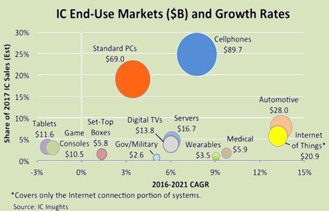
As established markets such as Smart Phones, Set Top Boxes, Computing and Game Consoles slow many companies are focusing their attention on the newly emerging Medical, Wearable and IoT markets. As the diagram below highlights these markets are predicted to grow at over 9% CAGR in the next few years.

However, to be successful in these markets will demand a markedly different design ethos. The more established markets were driven largely by performance criteria necessitating adoption of leading edge FinFET process technologies to deliver year on year step changes in compute horse power needed to satiate consumer expectations. The newly emerging markets are extremely cost sensitive and, more importantly, power critical. In the case of the IoT market for economic reasons many of these devices will be “fit and forget” hence necessitating extremely low power operation. Inclusion of high capacity Lithium Ion cells is precluded not only on cost grounds, but also on form factor. Addressing this challenge demands innovation from all eco-system partners; Foundries, IP Suppliers and EDA Vendors. Foundries continue to deliver low power variants of cost effective bulk technologies such as Ultra Low Power (ULP) and Ultra Low Leakage (ULL) flavours down to 22nm. There is also growing traction for FDSOI processes at both 28nm and 22nm. It is up to IP suppliers to exploit these advanced process technologies and create robust production worthy solutions capable of low voltage operation. Nowhere is this challenge more pertinent than the creation of low voltage SRAM.
LOW VOLTAGE DESIGN CHALLENGES
Operation at low and near threshold voltages needs special attention – not least the recharacterization of the logic cell library to adequately model the increased levels of variation caused by the exacerbation of process variability at low voltage levels. Liberty Variation Format with Moments (LVFM) originally developed to support leading edge process nodes is now being adopted as an expedient way of modelling behaviour as operating voltages are reduced. One area that has remained a challenge is that of embedded SRAM. Whilst the logic may be synthesised to operate at near threshold voltages thereby delivering the requisite power savings the inclusion of SRAM in such circuitry remains a fudge. Underlying this issue is the high-density foundry bit cell. This structure is optimised for packing density and is particularly susceptible to process variation. Statistical considerations mean that a significant minority of a bit cell population (of which there could easily be millions per chip) could be unduly “weak”. This “weakness” typically manifests itself in three major ways; low read current, write-ability and stability. Each of these issues will contribute to data loss and they are all greatly exacerbated by reducing the bit cell operating voltage rapidly introducing both read and write errors, Dual rail SRAM goes some way to ameliorate this problem by ensuring that the bit cell array is always correctly powered. However, the central problem of multiple supply rails and a ring of level shifters to interface to the memory remain. This approach can, of course, be made to work, but the impact on physical implementation, verification and timing closure means that a high degree of manual intervention is needed which brings a whole series of new challenges.
EVERON – A SINGLE RAIL ULTRA LOW VOLTAGE SRAM
The sureCore “EverOn” SRAM has been developed specifically for the demanding near threshold environment. Using patented “SMART-Assist” circuitry the memory has been silicon proven down to 0.6V across process corners and the full industrial temperature range (-40C to 125C) in a leading 40nm foundry ULP Logic and Embedded Flash process. Based entirely on the foundry 6T bit cell with no additional process options required the memory can be seamlessly integrated with low voltage logic and powered from the same supply. The challenges of weak bit cells as outlined above are effectively eliminated by the SMART-Assist circuits which always ensure that the bit cells being written to/read from are supplied with the optimal operating voltages for the duration of the write or read cycle. This architecture ensures that the performance of the SRAM tracks the logic and the whole SoC or a large subsystem can be developed as a single voltage domain greatly simplifying power routing and verification as illustrated below.

EVERON – FLEXIBLE SLEEP MODES
A key element of maximising battery life is power management. Often complex schemes are architected with on-chip Power Management Units (PMU), Dynamic Voltage & Frequency Scaling (DVFS) techniques as well as extensive clock and power gating depending upon system requirements. This adds further to the verification burden. Industry standard SRAM typically provides a number of sleep modes in order to help the system architect – usually light sleep, deep sleep and shutdown modes are regarded as normal with varying data retention capability, and varying recovery times to return to normal operation depending upon mode. However, from the system perspective where delivering every ounce of power saving is critical such a coarse grain approach to SRAM power saving often means spending considerable time analysing just how small particular SRAM instances can be made in order to deliver the lowest operating power profile to ensure mission critical code/data can be either executed or retained.
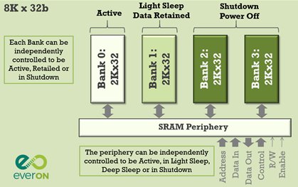
EverOn provides the system architect with much greater granularity of control as illustrated below.

The diagram above shows an 8Kx32b SRAM. All EverOn instances have four independently controllable banks – each being capable of being active, asleep (data retained) or shut down (powered off, no retention). In addition, the periphery is also independently controllable, either active, in light sleep (1 cycle wakeup), deep sleep (power supply drooped to cut leakage) or in full shutdown. Such granularity of control means system architects are no longer bound by the imposition of having to put the entire memory into one of several sleep modes. EverOn confers far greater flexibility and hence significantly eases power management challenges.
EVERON – PRODUCTION READY, AVAILABLE NOW
SureCore has invested considerable resources to ensure that the EverOn SRAM is production ready including an extensive verification environment to demonstrate adequate margins across PVT corners, corner silicon validation and successful completion of life tests.
Access to the compiler is via a web-based interface which generates the standard EDA model suite as well as product datasheets.
SUMMARY
As outlined earlier near threshold design methodology is delivering dramatic power savings for IoT, Medical and Wearable applications. Standard SRAM can be integrated into such a design environment but usually at the expense of architectural compromise and significant impact to physical and verification flows. The rich suite of power down modes EverOn provides delivers much improved flexibility into the hands of system architects. This coupled with a single supply rail solution and an industry first capability to track logic operating down to 0.6V means that genuine near threshold design methodologies can be rapidly and easily adopted. EverOn is the missing link in the quest to enable genuine ultra-low voltage design and provide SoC solutions that dramatically extend battery life
SURECORE : WHEN POWER IS PARAMOUNT
About sureCore
sureCore Limited is an SRAM IP company based in Sheffield, UK, developing low power memories for current and next generation, silicon process technologies. Its award-winning, world-leading, low power SRAM design is process independent and variability tolerant, mak-ing it suitable for a wide range of technology nodes. This IP will help SoC developers meet both challenging power budgets and manufacturability constraints posed by leading edge process nodes.
Related Semiconductor IP
- Ultra Low Voltage Embedded SRAM - TSMC 22ULL
- Ultra Low Voltage Embedded SRAM - TSMC 28HPC+
- Ultra Low Voltage Embedded SRAM - TSMC 40ULP
- Ultra Low Voltage (ULV) SRAM
- Samsung 28nm Low Voltage Single-Port SRAM Compiler
Related White Papers
- How Low Can You Go? Pushing the Limits of Transistors - Deep Low Voltage Enablement of Embedded Memories and Logic Libraries to Achieve Extreme Low Power
- Novel Trade-offs in 5 nm FinFET SRAM Arrays at Extremely Low Temperatures
- Low Power 7T SRAM Cell Scheme - ''Saving Write Zero Power''
- A 55-nm Ultra Low Leakage SRAM Compiler with Optimized Power Gating Design
Latest White Papers
- Breaking the Memory Bandwidth Boundary. GDDR7 IP Design Challenges & Solutions
- Automating NoC Design to Tackle Rising SoC Complexity
- Memory Prefetching Evaluation of Scientific Applications on a Modern HPC Arm-Based Processor
- Nine Compelling Reasons Why Menta eFPGA Is Essential for Achieving True Crypto Agility in Your ASIC or SoC
- CSR Management: Life Beyond Spreadsheets