Dynamic instruction set load-in method for Java SoC
By Zhirui Chen and Hongzhou Tan, Sun Yat-sen University Guangzhou China
Abstract :
There are varieties of embedded systems in the world, it’s a big challenge to optimized the instruction sets of SoCs according to different systems’ working environments. The idea of dynamic instruction set is a good method to achieve the embedded system’s re-configurability. This paper presents a convenient method for a Java processor to work with dynamic instruction set in the form of FPGA or ASIC. The costs of area, power and timing are trivial. Such idea is also reusable for other embedded system solutions.
1 Introduction
Dynamic instruction set is very useful in many embedded systems which can be widely used in different areas, and allows engineers developing more efficient instructions or changing the booting up codes. In the Java SoC field, most of the processors both in research or of commercial are designed using fixed instruction set. Only a few choose reconfigurable structures which have to be implemented in FPGA platforms, like the Lavacore[1]. This paper introduces a Java- processing chip with real dynamic instruction set inside. The architecture can be implemented not only in FPGAs, but also in ASICs. No matter what purpose an embedded system is designed for, the main idea for dynamic instruction set or say reconfigurable device is to use programmable logic within the SoC[1][2].
2 Processor structure
The Java processor used experimentally in this paper is called “Java Optimized Processor”-JOP[3]. It is a stack-based Java processor with four-stage pipelining. As shown in Figure 1, the four pipeline stages are bytecode fetch, microcode fetch, decode and execute.
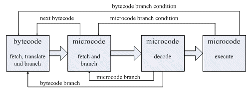
Figure 1. Four-stage pipelining
Bytecode is compiled Java instruction in binary form. It is the input for JVM[4] on computers or other Java processors like Jazelle from ARM[5]. Microcode is the native instruction of JOP. All bytecodes in a Java program are translated into series of microcodes first, and then the processor executes the translated local instructions—microcodes. This is the basic of the JOP mechanism (Figure 2).
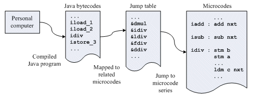
Figure 2. Translation from bytecode to microcode
JOP has different interfaces which allow it to communicate with outside. Considering the point that to design reusable IPs in this experiment, JOP has been modularized and re-constructed using AMBA[6] standard inside the chip. As a good result, the SoC can easily add or remove modules which are conformed to the AMBA standard.
JOP has been tested in different models of FPGAs. Inside the pipelines of JOP, several memory modules are used to implement Java method cache (bytecode RAM), microcode ROM, and stack RAM, which contain local instructions, jump table and variables, etc. Thus RAM-based FPGAs can fully handle the JOP implementation, according to the fact that memory contents can be changed easily by re-programming in FPGAs.
On the other hand, when JOP is implemented in SoC, which it should be, because the performance is much better in SoC then in FPGA for real-time embedded systems, the memory modules are fixed in SoC. ROMs’ contents are not changeable and the logic cannot be re-programmed to initialize the RAMs.
3 Dynamic load-in method
So far, there are three primary problems when JOP is implemented in a SoC. First, ROM stores all microcodes which are not fully translated the bytecode instructions yet, thus the ROM should be changeable so that microcodes can be extended. Second, when microcodes have been extended, jump table and related variables should be updated as well. Third, unlike FPGAs which can be easily re-programmed, SoC should seek another way to initialize the RAMs.
For the first problem, it can be simply solved by using RAM instead of ROM. As a result, all the memory modules in SoC are RAMs. If there is a convenient way to initialize or re-write all the RAMs in any time, the other two problems are solved already.
Before this JOP chip starting up, no softwares or programs can be executed, because RAMs that supposed to contain the instruction set and other run-time related information are empty. Thus RAMs can only be initialized before system booting up. In that case, a new hardware module should be included in order to load all the microcodes, jump table addresses, variables, etc. into the chip, so that the system can work properly, (shown in Figure 3).
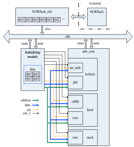
Figure 3. Initializing module in the chip
Figure 3 shows only part of the JOP logic, in order to illustrate the dynamic load-in method more clearly. The main CPU core is an AMBA master module which is tagged as “ahb_core”. Other controllers are AMBA slaves in this model, such as the NOR-flash controller. The indicated sub- modules in the main core are RAMs, with “jtbl” stands for jump-table RAM containing the addresses mapping to the microcode series, “ram” stands for the stack RAM containing all the constants and variables necessary for the system, and so forth. The pipelining stages are not shown in Figure 3.
The main core should be initialized before it can work properly after power-up, initializing module should be one of the AMBA masters, also the highest priority one, so that the system can automatically load in the contents to the RAMs when the system’s power is up.
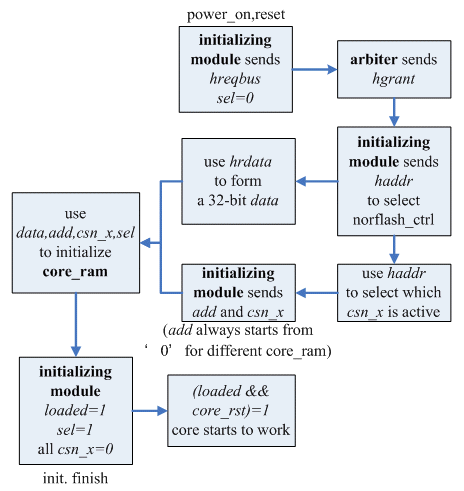
Figure 4. Initializing procedure
After system is power-on or reset, the initializing module (or named in “IM”) asks for permission to occupy the data and address buses. As IM has the highest priority, arbiter grants control to IM. Chip-selected signal of each on-chip memory module is controlled by IM, and so are the data and address signals of the memories. Data is loaded from external memory, which in this experiment it is a NOR-flash chip. The address signals in IM will start from “zero” after each on-chip memory finishes initialization. When all on-chip memories are done, a signal will be raised to release buses controlled by IM, then the main core (lower priority AMBA master) starts to work. Figure 4 shows the initialization procedure.
What IM has to do are, generates chip-selected signals, loads data from external memory, updates addresses related to on-chip RAMs, and sends booting up signals to the main core. The jobs are easy for IM which has a simple logic.
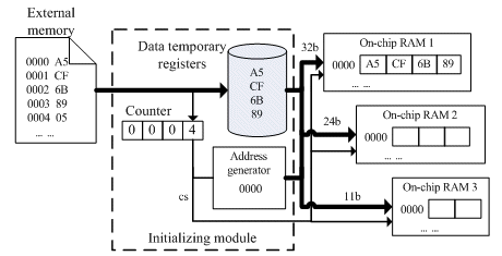
Figure 5. Main IM logics
The main logic of IM is a counter and some controlling signals generating logic. The controlling signals are generated according to the counter. Counting value will be increased by 1 each time an array of data (an array maybe 8-bit, 16-bit or others) is loaded. Though content is changeable in all RAMs, width and size of RAMs are fixed. Thus, controlling signals for RAMs can be generated correctly when the counter counts up to some certain numbers. For example, as shown in Figure 5, the on-chip RAM 1 is a 256×32bit memory. Assuming that the external NOR-flash is 8-bit width, the chip-selected signal of RAM 1 will be disabled and RAM 2 will be enabled for writing data when the counter counts up to 1024.
The address generator changes address relatively. As a RAM starts to be initialized, the address generator counts from “zero” and upwards. After a RAM is done, generator will clear back the address to “zero” for a next new RAM.
Not all the on-chip RAMs are in the same width, in order to meet the requirements of variable width of RAMs and storage resource saving, it is better to choose an 8-bit width external nonvolatile memory, such as NOR-flash to store the data. For RAM 1 in Figure 5, it should load four times to form a 32-bit data from external flash. For RAM 3, it should just load two times to form a 16-bit data then cut the high 5 bits out and finally get an 11-bit data.
There is a great advantage for embedded system using this initializing method. One can write a simple booting code or system testing code, then loads into the chip, and all codes can be modified easily when needed. This function will speed up the development and testing procedures of embedded system, as an operation system will be necessary normally when doing these jobs. For this experiment, code segments of clock management, power management, memory control initialization, etc. are implemented as part of the booting code.
4 Simulation
For simulation, an Altera Cyclone II[7] FPGA platform is used. The scales of AMBA-based JOP and IM are shown in Figure 6 and Figure 7 separately. According to the summary of logic elements that IM uses, a conclusion can be drawn that this module can be implemented in a SoC with small scale of circuits. The area and power problems caused by IM are trivial.
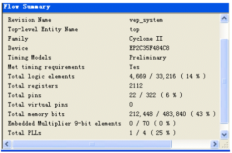
Figure 6. AMBA-based JOP cost summary
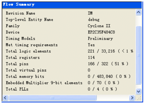
Figure 7. IM cost summary
Timing is not an issue either, as system cannot start to work before all the initial procedures are done. When the initial job is finished, IM will be no longer working and the module can be shut down, the actual working frequency of the chip is not affected by IM.
Also, the time period for initialization is short. The system is booting up already before one can even notice. In this AMBA-based JOP, there are totally 5698×8bits memory which have to be initialized as shown in Table 1. Assumed that the SoC initializing phase works at 50Mhz clock frequency. For reading an 8-bit data from external flash needs 4 clock cycles. The initializing time is 5698×4×20ns, that is 455.84us, even less than half of a microsecond.
Table 1. Memory modules inside JOP
| Name | Size | Needed bits |
| jtbl | 256×11bits | 256×16bits |
| offtbl | 32×11bits | 32×16bits |
| rom | 2048×10bits | 2048×16bits |
| ram | 256×32bits | 256×32bits |
| int_addr | 11bits | 16bits |
| Total bits: | 5698×8bits | |
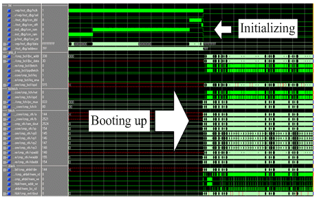
Figure 8. Initializing simulation waveform
In Figure 8, all memory bits inside the JOP main core are initialized, and different chip-selected waveforms can be seen. When the initial procedure is done, IM clock is shut, and JOP starts to work. A “Hello world!” Java program and Java threads scheduler have been tested in the AMBA-based JOP. IM does not affect the functional results compared to original JOP system.
5 Conclusions
In conclusion, IM hardly cost any area, power and timing expense from the summary above, but has such convenient and useful functions for embedded system. In addition, IM is designed into a standard-based IP module, like AMBA standard in this experiment. It’s easy to reuse the module in other embedded systems with the same standard.
Reference
[1] Bhaskar Bose, M. Esen Tuna and James M. Nagy, “LavaCORE Configurable Java Processor Core”, Aerospace Conference Proceedings, 2002. IEEE Volume 4, 2002 Page(s):4-1953 - 4-1959 vol.4.
[2] Fabio Campi, Mario Toma, Andrea Lodi, Andrea Cappelli, Roberto Canegallo and Roberto Guerrieri , “A VLIW processor with reconfigurable instruction set for embedded applications”, Solid-State Circuits Conference, 2003. Digest of Technical Papers. ISSCC. 2003, IEEE International 2003, Page(s):250 - 491 vol.1.
[3] Martin Schoeberl, “JOP : a java optimized processor for embedded real-time systems”, Wien,2005.
[4] Tim Lindholm, Frank Yellin, “The Java Virtual Machine Specification Second Edition”, Sun Microsystems, Inc. 1999.
[5] ARM Ltd., “Jazelle Technology For Execution Environments”, ARM DOI 0114-9/05.07.
[6] ARM Ltd., “AMBA Specification (Rev 2.0)”, ARM IHI 0011A, 1999.
[7] Altera Ltd., “Cyclone II Device Handbook”, Feb. 2008.
Related Semiconductor IP
- SHA-256 Secure Hash Algorithm IP Core
- EdDSA Curve25519 signature generation engine
- DeWarp IP
- 6-bit, 12 GSPS Flash ADC - GlobalFoundries 22nm
- LunaNet AFS LDPC Encoder and Decoder IP Core
Related Articles
- SoC Test and Verification -> Assertions speed processor core verification
- How to engineer efficient embedded Java applications
- Porting Legacy Code to Net Processor Designs
- Custom processors rev Java execution
Latest Articles
- TensorPool: A 3D-Stacked 8.4TFLOPS/4.3W Many-Core Domain-Specific Processor for AI-Native Radio Access Networks
- Assertain: Automated Security Assertion Generation Using Large Language Models
- VolTune: A Fine-Grained Runtime Voltage Control Architecture for FPGA Systems
- A Lightweight High-Throughput Collective-Capable NoC for Large-Scale ML Accelerators
- Quantifying Uncertainty in FMEDA Safety Metrics: An Error Propagation Approach for Enhanced ASIC Verification