Interlaken: the ideal high-speed chip-to-chip interface
By Comcores
As data consumption grows and chip designs evolve to meet this demand, Interlaken is the ideal high-speed chip-to-chip interface with efficiency, reliability and scalability.
Interlaken addresses modern chip-to-chip design challenges
System and chip designers are challenged like never before. The continuous growth in data consumption is driving demand for higher speeds and capacities, but designs also need to consume less power-per-bit at a lower cost-per-bit. Reliability is, of course, a key requirement, but not at the expense of efficiency and cost.
One of the chip design elements that is most critical is the chip-to-chip interface. Poor chip-to-chip interface design can lead to system bottlenecks and unreliable data transfers that can compromise the entire solution. Choosing the right chip-to-chip interface technology is therefore critical.
Interlaken provides a high-speed interface with efficiency, reliability and scalability. The design of the Interlaken interface ensures low power consumption and cost-per-bit without compromising on performance, reach or reliability.
Multiple design challenges
Efficiency
The challenge when connecting chips is to find an economic means of transferring data between chips on the Printed Circuit Board (PCB) implementation. This means as few pins and PCB physical connections, or trace-routes, as possible.
To achieve this, serial interfaces are preferred as they drastically reduce the number of pins required. Serial interfaces consume less power and are less sensitive to electro-magnetic interference compared to parallel connections. Serial interfaces have fewer connections that can be spaced effectively to reduce these effects. This increases the effective reach of the interface leading to longer trace-routes and more flexibility during design. This decreases the complexity and cost of PCB and chip design.
Reliability
One of the important requirements for chip-to-chip interfaces is that they need to be transparent. Data needs to be reliably transferred from one chip to another without relying on higher layer protocols.
First, the chip-to-chip interface needs to ensure that there is “bounded disparity”, which means that the number of ‘1’s and ‘0’s transmitted are as equal as possible. If not, a Direct Current (DC) offset is introduced that can affect coupling capacitors or transformers on the line. This can lead to challenges in identifying voltage levels accurately and retrieving clock data. To compensate for this, an effective block coding mechanism is needed that will reduce the “running disparity”, the difference between the number of ‘1’s and ‘0’s, as much as possible.
The next step is to ensure that bits have not been corrupted during transmission. An effective Cyclic Redundancy Check (CRC) for each data transmission can indicate if errors have occurred, while a Forward Error Correction (FEC) can be used to correct any errors.
Finally, it is desirable to ensure that the flow of data is controlled so that receiving chips are not overwhelmed, which can lead to packet loss. For bursty data that is switched to different locations, flow control can be extremely effective in managing data bursts and ensuring maximum throughput.
Scalability, Configurability and Reuse
In an ideal world, each application will have a chip-to-chip interface that is optimized for that specific application, but it is far more desirable to have an interface that can be configured and reused to meet different requirements.
Enabling the chip-to-chip interface to scale to meet different data rates enables maximum reuse across multiple designs and applications. In addition, the ability to configure the interface to fit different SerDes (Serializer/Deserializer [1]) lane configurations provides maximum flexibility in meeting application needs.
ASIC chip designs are often prototyped on FPGAs first. It is therefore desirable to have a chip-to-chip interface that can not only scale, but also migrate from FPGA platforms to ASIC designs with minimal impact. Today, FPGAs are often combined with ASICs, which requires chip-to-chip interfaces that can be implemented on either platform.
Introducing Interlaken
Interlaken provides a standardized serial interface that is agnostic of underlying SerDes implementations. It can also be configured to support multiple lane configurations.
Interlaken ensures reliable transfer of data over as few physical connections as possible. Interlaken provides mechanisms to ensure the integrity of data transfer as well as manage data flows to ensure that the chip is not overloaded. These mechanisms effectively increase the operational reach of Interlaken interfaces to allow longer chip-to-chip interfaces.
Interlaken inspired by XAUI and SPI4.2
Interlaken was introduced in 2006 by Cisco Systems and Cortina Systems to address the need for both a high-speed chip-to-chip interface and a reliable packet transfer mechanism. Available alternatives at the time were XAUI and SPI4.2 and both inspired the design of Interlaken, which combines the best of both.
XAUI
XAUI, or 10 Gigabit Attachment Unit Interface, was originally introduced in the IEEE 802.3ae standard for 10 Gbps Ethernet. In the standard, the 10 Gbps Ethernet protocol stack defined a new parallel interface between the MAC layer and the PHY layer called XGMII (10 Gbps Media Independent Interface).
System and chip designers needed the option of implementing the 10G MAC layer and PHY layer on different chips. However, the XGMII interface requires over 70 pins to connect the MAC and PHY. As a parallel interface with a high number of connections, the effective reach was relatively short at only 3 inches or 7.5 cm. This made XGMII an impractical chip-to-chip interface.
XAUI was defined as an alternative “XGMII extender” interface. XAUI is a serial interface that maps the parallel data of the XGMII interface to 4 serial interfaces operating at 3.125 Gbps. Each interface requires two connections leading to a need for 16 pins for full duplex operation, which is a dramatic improvement on the over 70 pins used by XGMII. The effective reach can be longer than 40 inches or 100 cm, but is specified normally to 20 inches or 50 cm.
It is this efficiency that inspired Interlaken designers to adopt a serial interface rather than a parallel interface.
The disadvantage of XAUI is that it is limited. While the 8b/10b block coding used in XAUI helps in improving running disparity, it does not remove the effects completely. A CRC is used to ensure that bits are transmitted correctly, but there is no flow control mechanism. This is not needed for communication between the MAC and the PHY, but can pose a problem if XAUI is used for other chip-to-chip applications.
SPI4.2
From a flow control perspective, the best example of an interface implementing this capability, at the time, was the SPI4.2 (System Packet Interface level 4, phase 2) interface published by the Optical Interconnect Forum (OIF) in 2003.
SPI4.2 was designed as a parallel interface between PHY devices and link-layer devices for 10 Gbps Ethernet, as well as OC-192 ATM and SONET/SDH.
One of the big advantages of the SPI4.2 interface is that a separate flow control interface is provided that allows the First-In First-Out (FIFO) buffer status of the receiver to be communicated back to the transmitter. The separate flow control interface enables the transmit and receive data flows to operate separately with their own flow control for each virtual port.
This ensures that the FIFOs at the receive side are not overloaded or starved. It also enables rate matching mechanisms, where the line rates on the transmit and receive sides can vary. This was the case with 10 Gbps LAN Ethernet, which operated at a different rate to 10 Gbps WAN Ethernet and OC-192.
Interlaken has adopted similar rate matching and flow control mechanisms as SPI4.2 using it as an inspiration for design.
Interlaken for high-speed chip-to-chip interfaces
Interlaken was conceived as the best of the XAUI and SPI4.2 implementations. It combines the serial, channelized interface of XAUI with the flow control capabilities of SPI4.2 to provide the ultimate high-speed chip-to-chip interface.
Interlaken provides efficiency
Interlaken is designed as a serial interface similar to XAUI and can achieve long reach using fewer physical pin connections. It makes it possible to use Interlaken in a variety of applications, from system-level chip-to-chip interfaces to chiplet-to-chiplet interfaces within a package.
In Interlaken, a meta-frame concept is introduced to control transmission of control and data words on each lane. For each lane, a set of words associated with the meta-frame are sent along with the payload of control and data words. These are:
- Synchronization: used to align lanes
- Scrambler State: used to synchronize the scrambler
- Skip: used for clock compensation
- Diagnostic: used for per-lane error checks and status messages
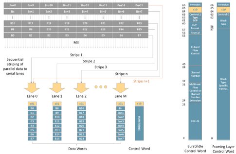
Figure 1: Interlaken striping and word format
Data is transmitted across the Interlaken interface in configurable bursts, like SPI4.2, which are a subset of the data to be transmitted. The minimum burst size, known as “BurstShort”, is 32 bytes divided into 8-byte increments known as “words”. An equivalent maximum burst size, named “BurstMax”, can also be configured. BurstMax is defined as a multiple of 64 bytes.
Similar to SPI4.2, the data word bursts are bookended by control words that provide additional information on the data being sent, as well as control information. The format of the control word is shown in Figure 1.
Each burst is associated with one of up to 65536 logical channels, which can represent ports or any other logical stream of data. This allows different data streams to be mixed while meeting tight latency requirements.
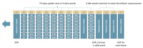
Figure 2: Transfer of 72-byte packet with BurstMax = 64 bytes and BurstShort = 32 bytes
An IP packet can be transmitted without interruption over several bursts. This is known as “Packet Mode”. Alternatively, segments from multiple packets can be interleaved. This is known as “Segment Mode”. The individual segments can be interleaved on different channels. The two modes enable the chip-to-chip interface to match application needs. For example, it might be more important to ensure that packets are not interrupted and sent in full using Packet Mode. Alternatively, for applications that need low latency, Segment Mode can be used to avoid head-of-line blocking and delays.
When the amount of data to be transmitted is less than BurstShort, Interlaken includes idle control words that can be inserted to meet the burst size requirements, as shown in Figure 2. When transmitting a specific packet, the start of the packet is indicated by a control word with a “Start of Packet (SOP)” field. The packet data is segmented into multiple 8-byte data words according to the configured burst size parameters with idle control words inserted as necessary.
The final control word contains an “End-of-Packet (EOP) Format Field”, which not only indicates the end of the packet transmission, but also how many bytes of the last data word are valid.
Interlaken provides several reliability mechanisms
Interlaken is designed to be completely transparent, thus providing different reliability mechanisms to ensure correct data transmission.
Better block encoding
First, Interlaken uses a more advanced block coding scheme to reduce running disparity as much as possible. A 64b/67b block scheme is used, where the 8-byte words to be transmitted are mapped or “striped” on a sequential basis to a 67-bit block. Using a larger block for encoding is more efficient and uses less bandwidth. At the receiver, the reverse operation occurs where the 67-bit block data is mapped to 8-byte words.
This is a similar mechanism to the 64b/66b block used in Ethernet implementations and defined in IEEE 802.3ae for WAN applications, but includes the addition of an additional inversion bit. The inversion bit indicates whether data has been inverted allowing mechanisms to reduce running disparity even further.
Similar to 64b/66b, the Interlaken implementation scrambles the 64-bit data to improve running disparity, but leaves two added “sync” bits unscrambled to enable control words to be identified.
Interlaken uses a 24-bit CRC in the control word that is calculated across all data in the burst across all lanes.
Flow control
One of the major advantages of the Interlaken interface is flow control. Inspired by SPI4.2, Interlaken implements a per-channel control mechanism, which enables the receiver to communicate backpressure.
The flow status of each channel is communicated using a single bit indicating either a ‘1’ for ‘XON’ state or a ‘0’ for ‘XOFF’ state per logical channel. Data can be transmitted on a channel as long as the flow control status is XON.
Interlaken provides the option of using a ‘calendar’ to indicate the status of all logical channels and the link at once. In the calendar, status is provided for the link as well as each logical channel with a single XON/XOFF bit.
Interlaken supports both out-of-band and in-band flow control allowing for efficient interface implementations. Out-of-band flow control requires separate pins while In-band flow control information is indicated in the flow control field of the control word.
With these flow control mechanisms, it is possible to meet the data flow requirements of each channel individually. Should the receive buffer of an interface become congested, the flow control can ensure that the transmission of data is managed to address this situation
An additional control feature is Rate Matching. This ensures that the data rate of the Interlaken interface is matched to the downstream service. This can be helpful in situations where two chip implementations operate with different clocks or there is a need to convert to different data rates.
One of the features of SPI4.2 that was not originally implemented in Interlaken was Hit-Less Bandwidth Re-Provisioning. It allows channels to be added or removed, channel priorities to be changed dynamically or channel bandwidth to be changed without affecting traffic on the interface.
In 2014, this capability was added with the Interlaken Dual Calendar Extension Revision 1.0. This allows two calendars to be defined, one active and one shadow calendar. A calendar selection bit (CAL_SEL) is added to the flow control word to indicate whether the active calendar or shadow calendar should be used (referred to as CAL0 and CAL1 respectively).
Multiple CRC checks
CRC checks are applied at multiple levels of Interlaken. First, a 24-bit CRC is calculated across all data in the burst, as well as the control word itself. At the meta-frame level, a 32-bit CRC is calculated across all words in the meta-frame. Out-of-band flow control is also protected with a 4-bit CRC.
These multiple levels of CRC checks ensure maximum data integrity. However, CRC checks can only indicate errors and not correct them. Therefore, in 2020, the Interlaken Alliance published the Interlaken Reed-Solomon Forward Error Correction Extension Rev. 1.1, which defines how the RS(544, 514) FEC can be used in Interlaken to provide additional data integrity protection.
In 2012, the Interlaken Alliance provided an extension called Interlaken Retransmit Extension Revision 1.2, which enabled buffered data retransmission in the event that a CRC error is detected.
Interlaken provides scalability
Because Interlaken is designed to be configurable and independent of the underlying physical lane implementation, it can be scaled to meet any requirement. This distinguishes Interlaken from both XAUI and SPI4.2 as both are based on a fixed number of connections.
For a chip designer, this is extremely useful. It means that the same Interlaken implementation can be configured to meet different chip-to-chip interface design requirements. For example, the chip-to-chip interface could be based on a single lane at full data capacity. Alternatively, it could be based on 4 lanes each operating at a quarter of the data capacity.
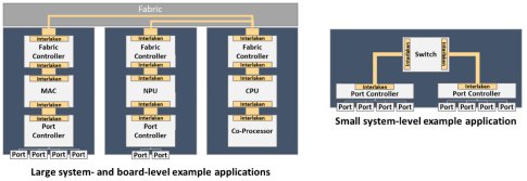
Figure 3: System- and board-level applications
When combined with the ability to define logical channels, the chip designer is provided with multiple configuration options that enable Interlaken to scale from single lane 10 Gbps connections to multi-100 Gbps connections. These scalability capabilities provide chip designers with reuse opportunities across multiple designs and applications.
Because Interlaken is standardized and independent of the underlying physical implementation, it allows a chip designer to design a chip-to-chip interface for an FPGA platform that can be reused should the design be migrated to an ASIC platform.
Interlaken applications
As a chip-to-chip interface that is independent of the underlying physical implementation, Interlaken can be used in multiple applications. Because of its configurability and scalability, it can be adapted to meet specific needs while ensuring a narrow, economic and reliable interface.
System-level applications
In a typical data processing system, the data processing units need to be connected to the data input/output logic.
For smaller systems, that can be a single pizza-box motherboard where MAC/PHY chips are connected directly to the data processing unit (e.g., CPU, NPU, GPU or similar) or a switch/mapper chip. In these applications, Interlaken can be used to connect the MAC/PHY chips to the data processing unit or switch.
The Interlaken logical channels can represent networking ports or switching ports, types of data, such as control or management data or different types of payload data, such as Ethernet or OC192.
Interlaken flow control and rate matching can be used in switch systems to manage the flow of input/output data based on the FIFO buffers for each switch port ensuring that no packet data is dropped in the system.
Because Interlaken is independent of the communication protocol or underlying implementation, the designer can choose where chip logic should reside. For example, the designer can choose how many sub-layers of the physical layer should be implemented close to the port and how many should be centralized in a separate chip. This can be seen in Ethernet implementations, but also in 5G RAN implementations with split-PHY eCPRI interfaces.
For larger systems, the data processing or switch units can be separated from the data input/output logic on separate plug-in boards connected over a backplane. Now, the Interlaken chip-to-chip interface needs to connect the same chips to each other, but must do so across the backplane. Thanks to the built-in reliability and relatively long-reach of Interlaken interfaces, this does not present a challenge. Figure 3 provides examples of system- and board-level applications.
Board-level applications
At the board-level, many of the same advantages can be reaped as at the system level. While network adapters have traditionally been focused on transferring data to and from central data processing units, modern adapters are increasingly offloading data processing tasks with more advanced capabilities.
This often includes data processing chips, and even switch chips, on the adapter based on ASICs, NPUs, GPUs and FPGAs. Adapter design has thus become more complex with more processing and memory chips on the adapter requiring high-speed chip-to-chip interfaces.
As board-level design is limited due to the size of the board (e.g., PCIe adapter, OCP mezzanine cards or motherboards), compact designs are important. Interlaken provides advantages such as reducing the cost, power consumption and complexity of the board design, because only a few physical lanes are required to be implemented.
Since board designs can involve multiple chips in the data path, Interlaken can be used to meet the individual requirements of each chip interface with respect to number of lanes and speed rates. Flow control and rate matching can be used to match data rates in applications where there can be clock or data rate discrepancies between chips.
Look-aside applications
In both system- and board-level applications, co-processing chips are used to offload specific tasks. This could be search engines, policing engines, cryptographic engines etc. Typically, they are focused on processing header information or specific types of packets or some other subset of the data being processed.
For these applications, the Interlaken Alliance has defined a lightweight version of the Interlaken protocol called Interlaken Look-Aside. This was published in 2008 as Interlaken Look-Aside Protocol Definition Revision 1.1. The Interlaken Look-Aside protocol is similar to Interlaken, but with the following differences:
- It is designed for fewer channels
- Packet Mode is used instead of segment mode
- Single-burst packets are used for short packets
- BurstShort minimum is reduced to 8 bytes
- A single reference clock with only 1 skip word
Using Interlaken Look-Aside feature, an even more compact and lightweight implementation can be adopted. For co-processor applications that are used to processing a small subset of the total data, the Interlaken interface can be used to directly connect the co-processor and main processor.
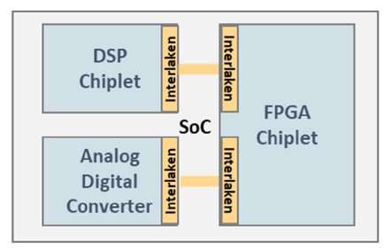
Figure 4: Chip-level applications
Chip-level applications
According to a recent report from PwC [2], global data consumption in 2020 increased 30.4% compared to 2019 and is expected to grow 26.9% per year until 2025. This requires higher speeds and capacities, which means bigger chips and greater power consumption. Power consumption is a major challenge for data centers and is as important as speed and capacity in decisions on which networking technology and chips to deploy. Space is also an issue, so compact solutions are important. The challenge, for both system and chip designers, is to minimize the cost, size and power consumption of systems and chips as much as possible.
This is leading chip designers to break up designs so that they can either be implemented on multiple physical chips or on ‘chiplets’, which are smaller chip dies that are combined with high-speed interfaces to form an efficient solution within a single package. This technique has been used by CPU manufacturers for some time and can also be seen in “System-on-Chip” (SoC) solutions, as shown in Figure 4. For chip designs that involve multiple separate chiplets, Interlaken can provide the ideal interconnecting interface. This is especially true for high-speed chip solutions.
For the user of the chip, it is important that it operates as if the implementation was on a single die. In other words, the interconnecting chiplet interface should not introduce any observable effects.
The reliability and flow control provided by Interlaken ensures that the interface is self-reliant as well as being efficient. It enables different chiplets with different requirements to be combined. Interlaken can configure the interface and control the data flow to match requirements. This allows efficient chiplet designs to be re-used in multiple packages.
Another chip-level application of Interlaken is System-on-Chip (SoC) solutions where FPGA logic is combined with hard-coded blocks or separate dies in the same package. A good example of this is SoC solutions supporting digital or even analog signal processing. The signal processing functionality can be provided on a separate die that is optimized for this kind of functionality. Interlaken provides an efficient and reliable interface for connecting blocks and separate dies with the FPGA logic.
Because the Interlaken interface is standardized and independent of the underlying implementation, it is also agnostic of the FPGA platform provider and can thus be used in solutions that need to support multiple FPGA vendors. The FPGA can also be migrated to an ASIC without major impact.
Suitable for a broad range of high-speed applications and reuse
Because of its configurability and scalability, a single Interlaken interface design can be reused to meet a broad range of applications making it an efficient and profitable design investment.
However, there is no need to invest in designing Interlaken interfaces, as pre-tested and verified implementations are already available that can easily be integrated into chip designs. Comcores Intellectual Property (IP) blocks can be used in both FPGA and ASIC designs and provide all the configurability and scalability that Interlaken is designed to deliver.
Comcores Interlaken IP can be used for a variety of applications making it a valuable investment that not only saves critical time and resources today, but also in future chip designs.
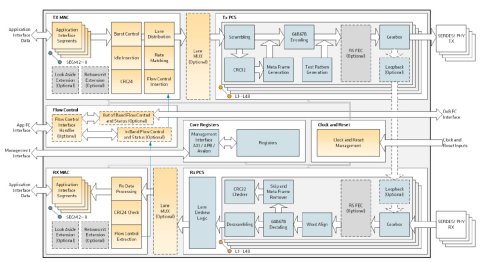
Figure 5: Comcores Interlaken Controller IP
Comcores Interlaken Intellectual Property
Comcores is the leading provider of reliable and efficient IP Blocks for Ethernet, Wireless and Chip to Chip interfaces including the Interlaken IP.
Complete solution with support for fast time-to-market
The Comcores Interlaken controller IP provides a complete Interlaken implementation including all extensions. The IP is designed for ease of integration enabling chip designers to quickly and easily implement and configure Interlaken chip-to-chip interfaces to suit their specific needs.
Comcores provides extensive documentation, reference design information with a complete simulation environment and Comcores engineers provide support throughout the design and bring-up process.
Highly configurable
In addition to the configurability expected of a complete Interlaken solution, Comcores also provides support for up to 48 SerDes lanes of 56 Gigabaud signaling rate enabling the Interlaken controller IP to deliver up to 2.6 Tbps per interface in both directions. The width of the SerDes interface can be configured from 10-bit or 67-bit interface widths.
An application interface is provided based on the ARM® AMBA® Credited eXtensible Stream (CXS) interface. The advantage of AMBA CXS as an application interface is that it is designed to support wide interfaces that can transfer packets at high data rates. This enables multiple packets to be merged into a single transfer if required.
The Comcores Interlaken controller IP can be configured to support various application interface widths of 256, 512, 1024, 2048, 4096 and 8192 bits. The number of interface segments can also be configured to be either 2, 4 or 8.
The Comcores Interlaken controller IP supports a variety of management interfaces to enable support for various chip designs and platforms:
- APB: ARM® Advanced Peripheral Bus interface, which is part of the Advanced Microcontroller Bus Architecture (AMBA®) and can be used in FGPA or ASIC designs
- AXI4-lite: part of the ARM® AMBA® AXI control interface and used by AMD®/Xilinx® for connecting to LogiCORE IP AXI interconnect core in an FPGA design
- Avalon: Intel®/Altera® interface for interconnecting components in an FPGA design
- I2C: Inter-Integrated Circuit serial communication bus interface
Simulation and testing environment
To enable fast time-to-market and ease of integration, Comcores provides extensive documentation and a simulation environment with test cases and test scripts. This includes a hardware test environment as well as RTL testbenches.
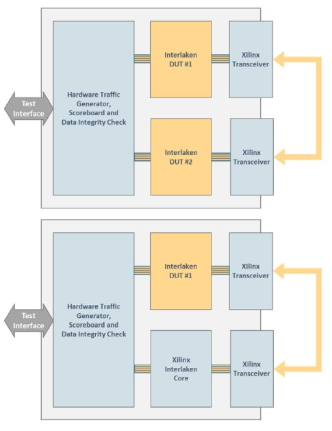
The current hardware test environment is based on a Xilinx Virtex-UltraScale VCU108 board (xcvu095-ffva2104-2-e) with External FMC loopback card. This enables two primary test cases to be implemented:
- Functional test: Implementation of two Interlaken interfaces in the same FPGA, which are then externally connected. A hardware traffic generator block drives data to both interfaces and then examines the received data on both application interfaces.
- Interoperability test: The same test is performed, but by replacing one of the Interlaken interfaces with a 3rd party Interlaken implementation, such as the Xilinx Interlaken core to test interoperability
Figure 6: Comcores Interlaken IP Core FPGA-based Test Environment
Future of Interlaken
As data consumption continues to grow, data center processing workloads and data network capacity needs to grow to meet demand. However, the challenge for today’s data centers is that low-cost-per-bit is no longer a sufficient performance goal. Low-power-consumption-per-bit is just as important. Raw speed and capacity are no longer enough; they need to be delivered with low power consumption.
This is forcing system and chip designers to re-think their approach. Instead of relying on CPUs as the main processing engine, a variety of alternatives are being used, such as ARM processors, NPUs, and GPUs, while there is an increase in the number of application-specific dedicated data processor solutions. Open RISC-V designs are now also available, including chiplets for integration in chip packages. SoC designs and disaggregated chip designs combining multiple optimized chiplets are also becoming more popular in an effort to meet stringent cost, speed, capacity and power consumption targets.
The common theme is a need to optimize how data is processed at every stage to ensure that an optimal system solution can be provided. Interlaken provides the ideal chip-to-chip interface to address these needs. As a highly configurable and scalable solution that is agnostic of the underlying physical implementation and whether the chip is FPGA or ASIC based, Interlaken can be optimized to meet the specific needs of modern system and chip designers.
Interlaken provides the further advantage of reuse in multiple applications and across platforms.
With the Comcores Interlaken IP Controller, chip designers have a complete, highly configurable IP block that can be quickly and easily integrated as well as verified with expert support throughout the process.
For more information on Comcores packaged IP solutions and access to Comcores Interlaken IP core visit: www.comcores.com or contact us at sales@comcores.com.
The hardware test environment can be controlled at the board level with the possibility of adding control via a UART console running a Linux environment. This can enable test configuration, launch and test result checks via user interface.
[1] A physical layer SerDes converts parallel data on multiple physical connections or lanes to serial data on one or more lanes
[2] Source: World Economic Forum (weforum.org)
Related Semiconductor IP
- Interlaken Look-Aside Intel® FPGA IP
- Interlaken Intel® FPGA IP
- Interlaken Controller
- Interlaken Verification IP
- Interlaken Synthesizable Transactor
Related White Papers
- High-Speed Serial fully digital interface between WLAN RF and BB chips
- AMS and High-speed Interface IP Design Enablement in GLOBALFOUNDRIES 65LPe Process Technology
- Why advanced DSPs running RTOSs are an ideal match for the IoT
- Common I/O design strategies for high-speed interfaces
Latest White Papers
- Breaking the Memory Bandwidth Boundary. GDDR7 IP Design Challenges & Solutions
- Automating NoC Design to Tackle Rising SoC Complexity
- Memory Prefetching Evaluation of Scientific Applications on a Modern HPC Arm-Based Processor
- Nine Compelling Reasons Why Menta eFPGA Is Essential for Achieving True Crypto Agility in Your ASIC or SoC
- CSR Management: Life Beyond Spreadsheets
