Complex SoC Verification using ARM Processor
By Mallesham Boini, eInfochips
Synopsis
Technology evolution, in part, has enabled the transition of multi-million gate designs from large printed circuit boards to SoC (System on Chip). The major advantages of SoC include low cost per gate, low power consumption, faster circuit operation, reliable implementation, smaller physical size and greater design security. With the ever increasing complexities and shrinking geometries the challenges involved with SoC design have grown substantially. The increased complexities of SoCs have led to significant increase in the verification efforts that are imperative to meet the timeto- market demands. Most companies have realized that traditional simulation methods no longer suffice SoC design verification for complete system level verification (hardware simulation and embedded software testing).
A verification environment with a mix of C tests for debugging (for embedded processor) and verilog test bench for monitors and automated checkers is used for successfully verification of an ARM based SoC design. This paper provides more detailed illustration that combines C (embedded test cases) and Verilog test bench for system level verification and also introduces verification techniques that helps in reducing verification time of SoCâs .
SoC Verification Flow
A typical SoC verification flow consists of three major tasks; modify, test and evaluate. The diagram below depicts the flow and the various processes carried out during SoC verification. Designers follow this iterative loop of modification, testing and evaluation until the verification objectives are met.
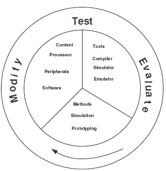
Figure 1: SoC Verification Flow
The size of the iterative loop circumference indicates time, which is the key in managing the throughput. The verification team aims at reducing the number of iterations or size of the loop.
In the test phase, verification methodology and tools have major impact on reduction of the Iterative Loop circumference. For the purpose of this article, we will discuss a typical SoC design that contains an ARM processor, memory, and custom RTL logic. The ARM processor communicates with memory and peripherals using an AHB bus interface.
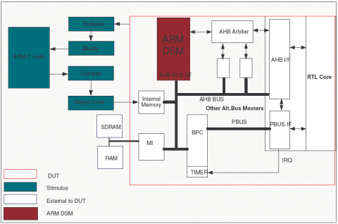
Figure 2: SoC Verification using ARM RTL model
The processor model is a design-signoff model (DSM) and all the peripherals and additional blocks in the design are included as RTL models (cores). Some of the RTL blocks / peripherals act as a secondary bus master to the ARM processor.
SoC System
The data to be processed is placed in RAM. Control and status information are passed back and forth from the RTL cores to the ARM processor via registers accessible over the ARM peripheral bus. In addition, there is a single interrupt from the RTL module/core to the ARM processor to indicate the completion of selected tasks. The register interface with the ARM processor is a 32-bit connection via the peripheral bus. The data interface is a 32-bit connection via the secondary bus master interface. Verification teams use the firmware running on the ARM processor as a part of the stimulus for verification using full functional processor models (DSM).
The software stimulus is compiled and the object code is loaded into the ARM processor memory. This is followed by simulation of the design in Verilog to discover all the bugs before the chip is taped-out to ensure right first time silicon success.
The ARM processor (C code stimulus) initializes and configures the RTL modules/blocks to process the data in the RAM by executing C code (Object code) through AMBA AHB Bus transactions. After the completion of initialization and configuration, the RTL module takes the ownership of AMBA AHB Bus and receives data from RAM. Once RTL module/block processes the data, it generates hardware interrupts to the ARM processor and updates its status registers for this operation. On receiving the interrupts the ARM processor checks the status registers of RTL core to validate the test case status (passed or failed). If the desired functionality is not achieved or test cases fail the iterative loop of modify, test and evaluate is followed.
Running firmware tests on the ARM DSM takes more time and is not a practical solution for large tests. The Firmware design and test teams are primarily interested in processor execution instructions. Also the hardware team suffers from the overhead associated with a full-functional model when their main interest is simply in the bus protocol and bus transactions. This demonstrates the increasing demand for better solutions from both the hardware and software teams perspective.
HW/SW Co-Verification and Test Generation
A traditional verification and test approach allows software verification only once the silicon is out from the foundry. This makes hardware and software debugging tasks sequential, increasing the product development time. The objective of Co-Verification is to make the hardware and software debugging tasks as concurrent as possible.
However, once the teams discover the benefits of co-verification they artificially believe that the design is bug free if the design runs all of the diagnostics, boots the operating system, and runs applications. Unfortunately, software changes frequently and there is little guarantee that the software exercises complete features and functions of hardware. A better approach to verification is by running a combination of software tests to verify the complete bus interface. Using the above ARM example and co-verification techniques this can be accomplished in two steps. First, it is possible to run software programs on an ARM co-verification model and capture the resulting sequences of AHB transfers created by these software programs as shown in Figure 3.
Secondly, the AHB transactions written in the form of a command file are used to drive a synthesizable bus functional model of the AHB protocol. These AHB commands file contains AMBA AHB transaction commands, sideband commands, and delay commands. The AHB transfer descriptions in this file have all the information needed to reproduce the sequence of operations as seen by the hardware design without requiring a full processor model.
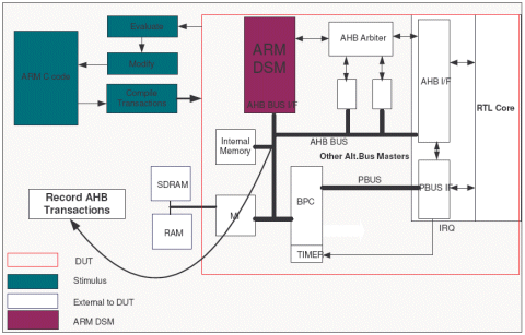
Figure 3: Capturing AHB Transactions to File
In the above application, co-verification is used to provide stimulus generation for a bus functional model. If a software test results in a possible hardware problem the hardware team can âreplayâ the transactions and debug without the use of co-verification and software debuggers. The sequence of AHB transfers also runs faster because the ARM processor is replaced by a bus functional model (BFM).
Figure 4 shows the processor model replaced with the synthesizable AHB BFM with the stimulus coming from the AHB command file. Once the full functional processor model is replaced with the BFM the Iterative Loop is manageable once again. The hardware designer replicates the sequence of AHB transfers and is able to analyze the results. This is done without the hardware team leaving the logic simulation environment.
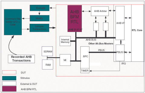
Figure 4: Reproducing the Error scenarioâs using captured Transactions
Random Test case Generation
To achieve full functional coverage its imperative to generate high speed stimulus. For high speed, the AHB BFM is recommended again. Transactions encapsulate the necessary address, data, and control information. Figure 5 shows transactions generated using a C program. With this architecture, tests can be directed, random, or a blend of both. The transaction files produced by software tests can be combined with random test generation to construct a comprehensive stress test for the hardware design.
The solution offers benefits from the synthesizable bus functional models that can also be used for simulation acceleration and emulation. The ARM subsystem is combined with other synthesizable models and in-circuit interfaces to create a complete verification environment. The C-API of the synthesizable AHB model also provides the necessary measurements for coverage. The verification team can use these metrics to adjust the random generation constraints and rerun the simulation to check the coverage improvement.
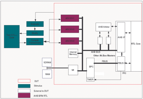
Figure 5: AHB Accelerated Iterative Loop
Coverage Analysis
To analyze the coverage of an AHB transaction model, an AHB coverage model, constraints applied to the AHB transaction model, and a reference model are introduced.
AHB Bus Interface Transactions
The AHB transaction model represents a single AHB transaction. To represent all possible AHB transactions and the possible delays before, during, and after each transaction requires a ten dimensional model consisting of the axes shown in Table below. For an ARM946 processor, only a 32-bit data bus using 212 bits total are required. 84 of these bits are specific to the protocol and the other 128 bits are specific to the delay values.
| AHB signal | Size |
| HWRITE | 1 bit |
| HBURST | 3 bits |
| HSIZE | 2 bits |
| HPROT | 4 bits |
| LENGTH | 10 bits |
| HADDR | 32 bits |
| HDATA | 32 bits |
| Pre-delay | 32 bits |
| Beat-delay | 64 bits |
| Post-delay | 32 bits |
| Total | 212 bits |
Table 1
AHB Coverage Requirements
The AHB coverage model is a subset of the AHB transaction model. The coverage model identifies the portions of the transaction model of most interest for specific hardware tests. Four signals of the transaction model are used directly: HWRITE, HBURST, HSIZE, and HPROT.
| AHB signal | Size |
| HWRITE | 1 bit |
| HBURST | 3 bits |
| HSIZE | 2 bits |
| HPROT | 4 bits |
| Any delay | 1 bit |
| Total | 11 bits |
Table 2
By collapsing the three signals related to delay into single axis with a single bit of data. The resulting five dimensional model uses eleven bits and is shown in Table above.
Constraints on AHB Transactions
Before generating random tests the signals of the AHB transaction model are constrained to deliver more focused tests. The transaction constraints used for the ARM Processor example are shown in the table 3 below.
| Hwrite | Hburst | Hsize | Length | Hprot | Haddr | Hdata | PreDelay | BeatDealy | PostDelay | Weight |
| 0 | 0,1 | 0,1 | 1-255 | 1-f | 0-ff | All | 0,1 | 0 | 0 | 1 |
| 1 | 2-7 | 2 | 0 | 0 | 100-1ff | All | 0,1 | 0 | 0 | 2 |
Table 3
There are two sets of constraints, indicated by the two rows in the table. The first row corresponds to the signals of the AHB transaction model and the last column provides a weight for each set of constraints. Each element in the table is a constraint specifying how a random value is chosen from the possible values for a signal. Each constraint takes the form of one or more fixed values, ranges, or sets. The random values generated for one type of weight are different than those for another weight.
Reference Data for Checking
Self checking tests are the best way to automate verification. The simplest way to do this is to use system data to check the validity of the design. To accomplish this, a reference model for the design is used. When a read occurs, the data returned from the reference model is sent to the BFM as the expected data during the read. The comparison is done in the BFM to maximize performance in simulation acceleration and emulation applications. A single bit reflecting the comparison is returned to the test program. The reference models can be implemented in C or Verilog for expected results.
Software Advantage
Using software as part of the verification, ensures the design will act in the same way as the final product. This stimulus will be ârealisticâ. That is it will put the design being tested through its typical operations. This enables support of system level co-verification of tests for the complete collection of components in hardware, software or combination of the two, uncovering problems that would never be found in isolation. The key in achieving the performance is to filter out code and data references that are not relevant to the operation of the hardware this is done by implementation of all monitors in Verilog. Also, using C code in Design Verification tests can be reused on the lab bench. Using software as a stimulus is faster and easier to create than writing stimulus in HDL.
Test case Development
Test case development involves writing test cases in C along with Verilog test bench. In order to allow synchronization between the C test code run by the ARM processor and the Verilog test bench, a âPorthole mechanismâ is supported in the simulation environment. Porthole mechanism allows using dedicated reserved addresses in the memory map. When writing to those addresses from the C test, the verilog environment will detect the address bus change and accordingly to the value of address and data written, will display the pre-defined message and activate the predefined verilog event. Monitors are used to snoop the ARM processorâs internal operations including register status that are implemented in verilog.
Conclusion
Improved system level verification approaches are needed for addressing verification of complex SoCâs. This requires verification teams to be effective in maintaining a small circumference on the Iterative Loop. AHB Bus transaction sequence coverage demonstrates a useful measure that applies to both co-verification used by the software team and test generation used by the hardware team, by effectively establishing communication between C (Embedded code) and verilog test bench.
AHB Bus Constrained random test sequences can quickly be created by understanding the transaction model and constraint specification. Coverage model definition assits in establishing verification goals. The interoperability between ARM co-verification and a synthesizable AHB BFM demonstrates impressive coverage results for random test generation using C (Embedded test cases) and Verilog test bench.
Related Semiconductor IP
- UFS 5.0 Host Controller IP
- PDM Receiver/PDM-to-PCM Converter
- Voltage and Temperature Sensor with integrated ADC - GlobalFoundries® 22FDX®
- 8MHz / 40MHz Pierce Oscillator - X-FAB XT018-0.18µm
- UCIe RX Interface
Related Articles
- Safety Verification and Optimization of Automotive Ethernet Using Dedicated SoC FIT Rates
- Smart Tracking of SoC Verification Progress Using Synopsys' Hierarchical Verification Plan (HVP)
- Low Power Design in SoC Using Arm IP
- SV-LLM: An Agentic Approach for SoC Security Verification using Large Language Models
Latest Articles
- An FPGA-Based SoC Architecture with a RISC-V Controller for Energy-Efficient Temporal-Coding Spiking Neural Networks
- Enabling RISC-V Vector Code Generation in MLIR through Custom xDSL Lowerings
- A Scalable Open-Source QEC System with Sub-Microsecond Decoding-Feedback Latency
- SNAP-V: A RISC-V SoC with Configurable Neuromorphic Acceleration for Small-Scale Spiking Neural Networks
- An FPGA Implementation of Displacement Vector Search for Intra Pattern Copy in JPEG XS