Clock Domain Crossing Glitch Detection Using Formal Verification
Kesava R. Talupuru, Sanjai Athi - MIPS Technologies
ABSTRACT
Current System-on-a-chip (SoC) designs contain increased levels of functional and structural complexities within a single system. With the integration of multiple designs, various clock domains are introduced. In this paper, we present a solution for finding clock domain crossing glitch using a combination of formal verification and static timing analysis techniques. This paper also talks about leveraging a formal verification tool to do sequential equivalence checking between a buggy design and bug fixed design if CDC glitch is found in late design stages
1. Introduction
Current System-on-a-chip (SoC) designs contain increased levels of functional and structural complexities within a single system, and with this integration of multiple design functionalities, various clock domains are introduced for the different portions of the SoC. Verification of these Clock Domain Crossing (CDC) designs presents a daunting challenge as the issues are related to transistor level analog effects in the circuits. The traditional RTL functional simulation verification techniques are insufficient to find these analogue issues. Some of the various CDC related issues are mentioned in [1, 2, 3, and 5]:
- Metastability issues caused by setup and hold-time violations of flip-flops.
- Jitter due to unpredictable delays across clock domains
- Functional issues due to convergence and divergences of crossover paths
- Functional issues due to divergence of metastable signals
Though static timing analysis (STA) is useful for timing closures, it requires manual inspection, assumes false paths, and is prone to errors. Gate-level timing simulations, which are also done as part of regular verification, may or may not find a timing violation, based on timing constraints and the implementation. If a gate-level simulation finds a timing violation for any path of a CDC signal, we cannot be sure whether or not there are any other potential violations in various CDC paths. Fixing the design at these late stages is also very risky.
CDC verification has been discussed in previous published papers; for example, [1, 4] talk about using CDC EDA tools, which utilize formal verification techniques to find missing synchronizers, re-convergence of synchronized signals, divergence in the crossover, etc. [5] talks about using System Verilog Assertions (SVA) to find CDC issues in simulation. Most of the papers assume that there is no combinatorial logic in domain crossing and in most cases combinatorial logic in clock domain crossing is not recommended. However, if combinatorial logic in domain crossings is required for meeting performance goals or for any other reasons, it is important to make sure that the glitches from the output of the combinatorial logic do not cause potential timing violations at the receiver. In this paper, we propose verification solutions to ensure glitch-free clock domain crossing signals when combinatorial logic is present in domain crossings for integral and nonintegral CDC designs.
2. Clock Domain Crossing Types
2.1 Synchronous Clock Domain Crossings
Clocks which have a known phase and frequency relationship between them are known as synchronous clocks [6]. The clocks originate from same clock root, and clock crossing between those clocks is known as synchronous clock domain crossing. Synchronous CDC is divided into several categories based on the phase and frequency relationship of the source and destination clocks as follows [6]:
- Clocks with the same frequency and zero phase difference
- Clocks with the same frequency and constant phase difference
- Clocks with different frequency and variable phase difference
- Integer multiple clocks
- Non-Integer multiple clocks
2.2 Asynchronous Clock Domain Crossings
Clocks which do not have a known phase or frequency relationship between them are known as asynchronous clocks [6]. The phase difference between the clocks is unpredictable, and there can be metastability issues if their active edges arrive very close to each other.
3. Glitch problem in CDC
Consider two synchronous clock domains which can be run at various integer and non-integer clock ratios, for example, 1:1, 2:1, 3:2, etc. The intent of the design is to avoid fractional cycletimes across clock domains, i.e., the timing constraint between flops across clock domains is at least 1 cycle-time of the fastest clock. In this paper, we consider non-integral 3:2 clock ratio as an example. Figure1 shows typical 3:2 clock ratio waveform.

Figure1: Typical 3:2 clock ratio waveform
In the waveform, we can see the possible time periods between posedge to posedge of faster clock (Clk1) to slower clock (Clk2) in a 3:2 clock ratio are 1.5T, 1T, and 0.5T, where T is the cycle time of the faster clock. The design intent is to have a set-up time of at least 1T cycle time. Consider a sample CDC design snippet as shown in Figure 2a. Flops F1 and F2 are in faster Clk1 clock domain. Flop F3 is in slower Clk2 clock domain. Signals T1 and T2 are launched by Clk1 clock domain, and will go through combinatorial logic before captured by Clk2 clock domain. As the design intent is at least 1T cycle time, Flops F1 and F2 in Clk1 domain cannot launch at 0.5T edge shown as X in Figure 2b. When data is transferred from Clk1 to Clk2 domain at clock edge X, there is a possibility of glitch which cannot be seen in functional simulation, but will appear in the hardware. Figure 2b, shows the timing diagram where a glitch can happen in the real circuit with 3:2 clock ratio. In Figure 2b, say at clock edge X, inputs T1 and T2 of AND gate changes from 1->0 and 0->1 respectively at the positive edge of Clk1, then this should effectively maintain a value of 0 at the output of AND gate. But, if T1 and T2 arrival times are different because of real circuit delays, then there may be a glitch at the output of the AND gate before the AND gate output T3 settles down to 0. So, if Clk2 clock edge which is 0.5T later were to sample the output of the AND gate, then there is a possibility that this edge would capture the glitch generated at the AND gate output which can cause a possible functional failure of the design. This glitch can be avoided if Flops F1 and F2 in Clk1 domain do not launch at clock edge X. By using the combination of formal verification and static timing analysis (STA), we prove that for all clock ratios, a possible glitch generated in one clock domain cannot cause a timing violation in the other clock domain.
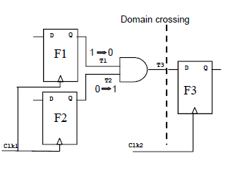
Figure 2a: Sample CDC design
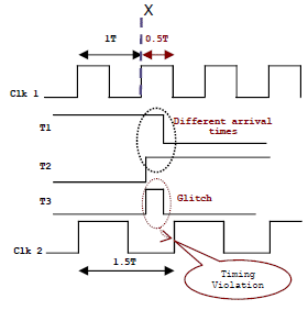
Figure 2b: Glitch in CDC for 3:2 clock ratio
4. Formal Verification
[7, 8] talk about modeling the effects of CDC glitch in functional simulation by introducing pseudorandom delays in CDC signals in the synchronizers. [4] talks about the various limitations of pseudorandom delays: all the effects of CDC glitch are not modeled, results are difficult to predict as glitch is introduced randomly, and hard to debug. To address the pseudorandom method limitations, [4] proposes inserting glitch logic, writing assertions around that, and proving those assertions by using formal verification techniques. [4] assumes that there is no combinatorial logic present when signals cross the domains. In this paper, by using formal assertion based verification, we verify that glitch cannot happen even if there is combinatorial logic present across the clock domain for integral and non-integral clock ratios.
Figure 3a, represents a sample CDC design with Clk1 and Clk2 domains, and having a combinatorial logic across the domains. These two domains are running at 3:2 clock ratio with Clk1 being the faster clock. Figure 3b, represents a sample waveform for 3:2 clock ratio. STA tuned for 1T timing constraint can detect the glitch for 1T and 1.5T cycle paths. For 0.5T paths, STA checks will result in many false violations. So, for 0.5T paths we need to use formal verification to prove that glitch cannot happen. In order to achieve this, we need to first generate a sync strobe as shown in Figure 3b. Sync strobe will be active for 1T and 1.5T paths indicating that Clk1 domain flops can launch. It is de-asserted for 0.5T paths indicating that Clk1 domain flops cannot launch. So, when sync strobe is low, if we write a data stability assertion at the end of the combinatorial logic (Signal T5) to check that the current value of signal T5 at clock edge X is equal to its value one cycle before. The system verilog assertion (SVA) is shown below to check the stability of signal T5 at clock edge X where 0.5T is the timing between Clk1 and Clk2 clock edges.
!sync_strobe |=> (T5 == $past(T5)));
If formal verification proves the above property exhaustively, then it is guaranteed that the Clk1 domain flops do not launch at 0.5T path, and as a result there won’t be any glitch in the Clk2 domain. The above property needs to be instantiated for all the signals that cross the domain, and need to be proven using formal verification to achieve a glitch free CDC. Writing the assertions at the very end of combinatorial logic can lead to a false positive formal proof which is described in section 5.
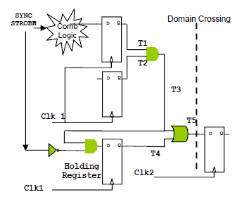
Figure3a: Sample CDC design
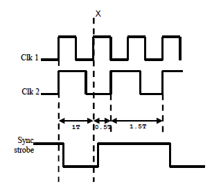
Figure3b: 3:2 clock ratio waves with sync strobe
5. Avoiding False Positives
We have to be very careful about at what points in the cross domain logic we need to write the SVA assertions to avoid false positives. In Figure 3a, if the assertion is written to check the glitch at the end of the combinatorial logic (signal T5), then we mask out the potential glitch at RTL level. For example, in Figure 3a, at 0.5T cycle path if inputs T1 and T2 of AND gate changes from 1->0 and 0->1 respectively at the positive edge of Clk1, then this should effectively maintain a value of 0 at the output of AND gate (signal T3) as the inputs change at the same time in RTL simulation. This behavior is shown in Figure 4, where T1 and T2 arrive at same time, and as a result there is no value change in T3 and T5. So, if the assertion is written for Signal T5, then even though the Clk1 flops launched at 0.5T path, signal T5 value looks stable, and the assertion is proven correct. As a result of this we get false positives in formal proofs at RTL level.
In order to avoid false positives, we leverage STA again to find all flip-flop outputs that drive the domain crossing combinatorial logic. For example in Figure 3a, signals T1, T2, and T4 are the outputs of Clk1 domain launch flops. We then write properties at those flip-flop outputs to make sure that there is no signal value change at 0.5T path for all those launch flop outputs, and as a result there won’t be any glitch. If formal verification falsifies the assertion, then there is real potential for the glitch to occur in the hardware. The same checks can be extended to 1.5T and 1T paths also. The sample code for getting all the launching flop outputs using STA is shown below:
foreach_in_collection tim_path [get_timing_paths -group CLK2 -max_paths 10000] {
# Startpoints
set sp_clk_pin CLK1
set flop_out_pin [get_pins -filter "pin_direction==out" -of_objects [get_cells -of_objects CLK1]
echo "Flop outputs: [get_object_name $flop_out_pin]" } }
Once we get the list of launch flop outputs, we scriptify the list to generate assertions like below for the design in Figure 3a:
@(posedge Clk1) disable iff(reset)
!sync_strobe |=> (T == $past(T));
endproperty
Sig_T1: assert property (Check_Signal_Stability_at_0.5T_edge(T1));
Sig_T2: assert property (Check_Signal_Stability_at_0.5T_edge(T2));
Sig_T4: assert property (Check_Signal_Stability_at_0.5T_edge(T4));
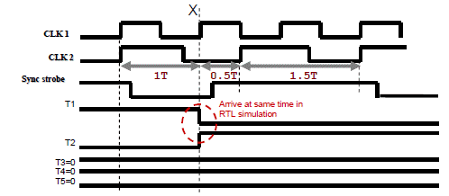
Figure4: False positive case waveform
6. Sequential Equivalence Checking
In this paper, we also discuss about the approach to consider if an RTL bug fix needs to be made for timing, but not for functional reasons. We recommend the following steps in order to obtain a high level of confidence in the bug fix, and to minimize the impact on tape-out schedules when the glitch is found in late design stages, such as gate-level simulation:
- First reproduce the glitch at the RTL level by writing assertions as explained in section 4, and proving that the glitch exists using formal verification.
- Prove that the glitch cannot happen by using the same assertions, and exhaustively proving it in a formal verification framework, for the bug-fixed RTL.
- As the old and new RTL should be functionally equivalent, we must prove that the two designs are functionally equivalent, and that the bug fix did not cause any unwanted side effects. To prove equivalency between the two RTL designs, we cannot make use of EDA tools like Conformal/Formality as they require one-to-one matching flip-flops, which may not be available after the bug fix. To overcome this limitation, we propose a solution that provides sequential equivalency checking by leveraging regular formal tools like Synopsys Magellan, Cadence IFV, etc. To achieve this, we form a Miter circuit as shown in Figure 5, between the corresponding outputs of the two RTL designs, and write a property at the output of each miter to prove that the miter output is never one.
assert property (@(posedge clk) OpN != 1);
After an exhaustive formal search, if the miter output is never one for all outputs of the design, then the two designs are functionally equivalent. With the above steps, we obtain a high-level of confidence in the bug fix before we run the large and time-consuming regression suites.

Figure 5: Sequential equivalence checking with miter formation
7. Results
Table 1 shows the results for one of the CDC designs. The design is verified for 1:1, 2:1, and 3:2 clock ratios. The assertions are automatically generated using scripts based on the launching flop output signals generated by STA.
| CDC Design | # Flops | # Gates | # Assertions | Time (Seconds) |
| 3:2 Clock Ratio | 3650 | 59300 | 80 | 240 |
| 2:1 Clock Ratio | 3650 | 59300 | 80 | 16 |
| 1:1 Clock Ratio | 3650 | 59300 | 80 | 10 |
Table 1: Sample CDC design formal proofs run time
8. Summary
In this paper, we have presented the glitch issue in CDC designs, and how to tackle the glitch issue using formal verification and static timing analysis. We also presented how to leverage regular formal tools to do sequential equivalence checking. By using these techniques, we can avert costly silicon failures in clock domain crossing designs.
9. References:
1. Cadence Technical Paper, Closing the loop on clock domain functional implementation problems.
2. Clifford E. Cummings, “Synthesis and Scripting Techniques for Designing Multi- Asynchronous Clock Designs,” SNUG-2001.
3. Carver Mead, et al., “Introduction to VLSI Systems,” Addison Wesley, pp. 237-242, Oct. 1980
4. Tai Ly, Neil Hand, Chris Kwok, “Formally verifying clock domain crossing jitter using assertion based verification”.
5. Mark Litterick, Pragmatic simulation based verification of clock domain crossing signals and jitter using system verilog assertions, DVCON 2006.
6. Saurabh Verma, Ashima S. Dabare, Atrenta, Understanding Clock Domain Crossing Issues, EETimes 2007
7. Janick Bergeron, “Writing Testbenches, Function Verification of HDL Models,” Kluwer Academic Publishers, 2000
8. Prakash Rashinka, et al, “System-on-a-chip Verification. Methodology & Techniques,” Kluwer Academic Publishers, 2001
Related Semiconductor IP
- NPU IP Core for Mobile
- NPU IP Core for Edge
- Specialized Video Processing NPU IP
- HYPERBUS™ Memory Controller
- AV1 Video Encoder IP
Related White Papers
- Understanding Clock Domain Crossing Issues
- The Challenge of the Clock Domain Crossing verification in DO-254
- Multiple clock domain SoCs: Verification techniques
- Clock domain modeling is essential in high density SoC design
Latest White Papers
- Transition Fixes in 3nm Multi-Voltage SoC Design
- CXL Topology-Aware and Expander-Driven Prefetching: Unlocking SSD Performance
- Breaking the Memory Bandwidth Boundary. GDDR7 IP Design Challenges & Solutions
- Automating NoC Design to Tackle Rising SoC Complexity
- Memory Prefetching Evaluation of Scientific Applications on a Modern HPC Arm-Based Processor