CE-ATA: Consumer Electronics Storage Technology Introduction and Hardware Design Challenges
Cairo, Egypt
Abstract:
The evolution in consumer electronicsâ applications has resulted in an enlargement of the digital data amount. The expansion of digital information in consumer electronics has stimulated the industry to produce new innovative storage technologies to harvest the ramping demand, and requirements of the storage capacity in consumer electronics domain.
CE-ATA [1] (Consumer Electronics - Advanced Technology Attachment) is the industryâs response for providing an optimized standard interface for SFF (Small Form Factor) storage solutions in handheld, portable and consumer electronicsâ applications.
This paper introduces an overview of the state-of-the-art technology underneath the hood of the CE-ATA industryâs storage standard. The paper addresses an explanation of the standard which leverages existing and proven technologies such as ATA and MMC (MultiMediaCard). The paper presents an overview of the various layers of the protocol used for communication between the host and a SFF storage device.
The paper continues to project the standardâs technology in real design cases of host and device controller IP cores. The paper outlines the hardware design architecture of the CE-ATA host and device controller IP cores that implements the CE-ATA standardâs functionality and performance requirements, and presents suggested solutions for the CE-ATA technology hardware design challenges.
The paperâs ultimate objective is to construct a primitive âknow-howâ baseline for the CE-ATA storage technology supported by hardware design casesâ overview of CE-ATA host, and device controller IP cores for integration into consumer electronicsâ SOCs
SECTION I 2
This section presents an introductory overview of the CE-ATA storage interface. It introduces the need for CE-ATA in consumer electronics storage integration as an optimized interface for that purpose, and shows how CE-ATA builds on the proven MMC interface and ATA command set to enable fast time-to-market solutions.
NEW INTERFACE REQUIREMENTS
Flash technology has dominated a large portion of the mass storage in consumer electronic devices. Common Flash interfaces, like MMC, have several advantages such as low pin count, low voltages, and compact size which lead to efficient integration of Flash in consumer electronics applications.
CF+ 3(Compact Flash +) is the current interface for SFF hard disk drives. CF+ is the traditional Parallel ATA4 interface crammed into a small space. CF+ has roughly fifty pins, a large physical connector size, and high-voltage signaling making it poorly suited to consumer electronics applications where space is at a premium.
The CE-ATA interface was created to address the need for a SFF hard disk interface as efficient as current interface options for Flash. CE-ATA addresses the need for an optimized interface specifically for SFF hard disk drives.
OPTIMIZED FOR SFF HDD
CE-ATA is an optimized interface for handheld and portable consumer electronics. CE-ATA addresses power requirements of this market segment by having a small number of low voltage transceivers with low static power consumption.
CE-ATA has scalable transfer rates up to 52 MB/s appropriate for performance requirements of SFF hard disk drives well into the future.
CE-ATA has low pin count with six or ten interface signals, depending on data transfer rate requirements. CE-ATA includes a streamlined ATA command set and a simple transport layer protocol.
CE-ATA leverages existing proven technologies. CE-ATA uses the ATA command set that is used in all desktop and mobile hard drives today. The ATA protocol is layered on top of the MMC5 electrical interface, which is broadly used in Flash memory card applications today. Building on these technologies enables fast time-to-market for initial products.
MMC COMMANDS IN CE-ATA SCOPE
CE-ATA utilizes five MMC commands during the course of normal execution. Hard resets are performed using the âGO_IDLE_STATE (CMD0)â, Aborting an ATA command is done by issuing âSTOP_TRANSMISSION (CMD12)â, byte-wise access to the ATA taskfile register is achieved using âFAST_IO (CMD39)â, issuance of an ATA command or access to the status and control registers is executed by âRW_MULTIPLE_REGISTER (CMD60)â, ATA command data transfer is achieved using âRW_MULTIPLE_BLOCK (CMD61)â.
CMD60 and CMD61 are MMC commands newly defined by CE-ATA for efficient ATA command execution. CE-ATA utilizes the same MMC command sequence for initialization as traditional MMC devices. The ATA operation occurs within the MMC âTRANâ state.
ATA PROCESSING ON MMC
CE-ATA maps the streamlined ATA command set onto the MMC interface. The ATA taskfile is mapped onto the MMC register space starting at MMC address zero as outlined in Figure-1. 48-bit addressing is accommodated from the start to accommodate future capacity growth, and to ensure that large transfers can be done. Transferring a single song from the device typically requires more than 128KB of data which is the maximum transfer size with only 28-bit LBA addressing.
| Register Address | ATA Register (8 bits) |
| 0 | Reserved |
| 1 | Features (exp) |
| 2 | Sector count (exp) |
| 3 | LBA low (exp) |
| 4 | LBA Mid (exp) |
| 5 | LBA High (exp) |
| 6 | Control |
| 7 | Reserved |
| 8 | Reserved |
| 9 | Features (write)/ Error (read) |
| 10 | Sector Count |
| 11 | LBA Low |
| 12 | LBA Mid |
| 13 | LBA High |
| 14 | Device/Head |
| 15 | Command (write)/ Status (read) |
Table 1- ATA taskfile mapping to MMC register space
RW_MULTIPLE_REGISTER (CMD60)
Allows multiple registers to be read/written in a single transaction sequence. Using CMD60 an ATA command can be issued with a single MMC command. Alternatively, software may have to execute up to thirteen individual taskfile register writes with FAST_IO in order to issue a single ATA command.
RW_MULTIPLE_BLOCK (CMD61)
CMD61 is used to transfer the data for an ATA command (like READ DMA EXT). Data transfer for media access commands must be multiples of the CE-ATA sector size that is 4KB minimum. Each transfer is broken into multiple MMC data blocks that are 512 bytes, 1KB or 4KB in size as negotiated between the host and the device.
REDUCED ATA COMMAND SET
CE-ATA only requires support for a small subset (less than 1/10) of the ATA command set. The reduced command set consists of (IDENTIFY DEVICE, READ DMA EXT, WRITE DMA EXT, STANDBY IMMEDIATE, FLUSH CACHE EXT).
A streamlined command set with few options reduces firmware and implementation complexity, and simplifies validation.
ATA COMMAND EXECUTION, INTERRUPTS DISABLED
Polling by CMD39 is used for reading the ATA status register when interrupt disabled (nIEN=1 in ATA Control register).
For instance to read 8 KB of data, host issues READ DMA EXT ATA command with RW_MULTIPLE_REGISTER for 8KB of data. Host reads the ATA status register with CMD39 until DRQ bit is set.
Host issues RW_MULTIPLE_BLOCK to read data. Finally, Host polls the ATA status register with CMD39 until BSY bit and DRQ bit are cleared. The polling projects significant inefficiency into protocol. Figure-1 depicts command/response sequences.

Figure 1- ATA command/response sequence, polling
INTERRUPT MECHANISM
CE-ATA eliminates interruptâs overhead with an efficient interrupt mechanism that doesnât add an interrupt pin as of reduction target of pin count.
The command line is quiescent after the receipt of CMD61 response. Hence, device sends an interrupt over the command line after the command completion.
This interrupt is defined as âCCS-Command Completion Signalâ. MMC resets are only executed by commands, and avoidance of collision on command line when CCS signal is outstanding is accomplished by using CCSD âCommand Completion Signal Disableâ from the host.
CCSD consists of four consecutive zeros followed by one but CCS is single zero. Hence, CCSD disables the interrupt safely with the avoidance of the push-pull transceivers driving in different directions.
ATA COMMAND EXECUTION, INTERRUPTS ENABLED
The same (READ DMA EXT) for 8KB of data can be executed when interrupts enabled (nIEN=0 in ATA control register) with CMD60 issuance to write ATA taskfile registers. Only one CMD61 follows for 8KB data transfer, then device issues CCS signal to notify the host with an ATA command completion. Figure 2 outlines the command/response sequence for this example.

Figure 2- ATA command/response sequence, Interrupts Enabled case
MEDIA ACCESS COMMANDS
CE-ATA uses one data transfer mode, DMA. (READ/WRITE DMA EXT) commands are the only media access commands. Alignment/Granularity restrictions accommodate the 4KB CE-ATA sectors while providing seamless compatibility with ATA 512 bytes sector size.
Host should align transfers to the device reported sector size. (Sector Count) register bits 0,1,2 are zeros for granularity, and (LBA Low) register bits 0,1,2 are zeros for alignment of 4KB sector size.
CE-ATA DEVICE INITIALIZATION AND DISCOVERY
CE-ATA uses the traditional ATA notion of a signature to signify its presence. The device places the signature in ATA task file registers after power up or reset. Host reads the signature to determine the device CE-ATA compliance.
STATUS AND CONTROL REGISTERS
CE-ATA adds a set of 32 bit registers used for additional status and control information. For instance, (scrTempC) register informs about current temperature reading, and (scrStatus) register provides status information of the device. The SCR registers addition makes the SMART feature of ATA unnecessary in CE-ATA domain.
SECTION II: CE-ATA HOST/DEVICE IP CORES OVERVIEW 6
This section presents CE-ATA standardâs technology in real design cases of host, and device controller IP cores. It outlines the hardware design architecture of the CE-ATA IP cores that implements CE-ATA standardâs functionality, and performance requirements.
CE-ATA HOST/DEVICE IP CORES FEATURES
The host/device IP cores are compliant with CE-ATA revision 1.1, and MMC revision 4.1. The cores support 1, 4, 8 bit(s) MMC data lines, provides CPU side interface through AHB Target interface, provides DMA interface though AHB Master interface.
The data buffers have programmable threshold. The cores implement CRC-16 for Data lines, and CRC-7 for command line. The Power-on- reset is done with hard coded state machine. Clock divider is included for MMC clock generation. The host core emulates CE-ATA device taskfile and SCR registers.
CE-ATA HOST/DEVICE HARDWARE ARCHITECHTURE
The main building blocks of the hardware architecture of the host/device cores consists of MMC bus adapter module, MMC layer module, ATA layer module, CE-ATA controller module, DMA controller module, and AHB master and target interface modules. Figure3, 4 depict the IP coresâ hardware architecture respectively.
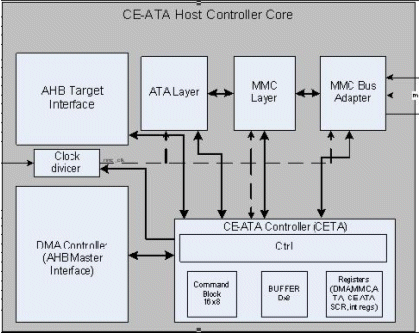
Figure 3 â CE-ATA host Controller IP core
The right hand side of figure 3, 4 interfaces the cores to the MMC bus interface, and the left hand side has two AHB interfaces, master and target. The target interfaces the core to the host CPU, and the master interfaces the core to an external memory. The MMC bus adapter, MMC layer, and ATA layer modules run on the MMC clock frequency, while the rest of the logic run on the main system clock. Hence, a synchronization layer between the AMBA7 AHB modules, and the MMC/ATA modules handles synchronization between clock domains of system and MMC clocks.
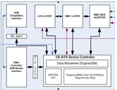
Figure 4 â CE-ATA Device Controller IP core
Section III: CE-ATA HOST/DEVICE IP CORESâ BUILDING MODULES
This section outlines the main building modulesâ features, functionality and interfaces of CE-ATA host, and device controller IP coresâ hardware architecture in sight of the CE-ATA digital protocol context.
The standard specification describes the protocol for implementation of the device side. Based on that, and the analogy between host, and device architecture, the next overview is mainly about CE-ATA device IP coreâs architecture building modules.
MMC BUS ADAPTER MODULE
The MMC bus adapter handles the communication on the MMC bus. It performs any serial-to-parallel or parallel-to-serial conversion on the data and command pins. It generates, and checks the CRC for both data and command according to the polynomials specified in the MMC specification.
It has a read and write FIFOs.
Figure 5 illustrates the block diagram for MMC Bus Adapter. The right hand side interfaces the module to the MMC bus command and data lines. The left hand side interfaces to the MMC layer and CE-ATA controller module.
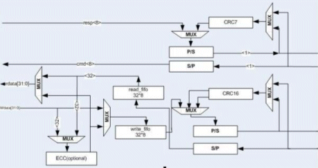
Figure 5 â MMC Bus adapter module
MMC LAYER MODULE
The MMC layer module implements the device MMC state machines as specified in CE-ATA specification. These state machines implement the MMC commands as specified in CE-ATA and MMC specifications (CMD60, CMD61, CMD39, CMD12, and CMD0). There will be 2 independent state machines: command and data state machines.
These state machines functions on the command received from the MMC adapter module, after being decoded. In addition to these commands, any commands needed during power-up or reset communication between the MMC host and device, as well as accessing the mandatory card registers (OCR, CID, CSD, EXT_CSD, RCA and DSR) are implemented. All the negotiations with the MMC host in order to get to the MMC transfer state (MMC_TRAN) are handled with this module.
Figure 6 illustrates the block diagram for MMC Layer module.
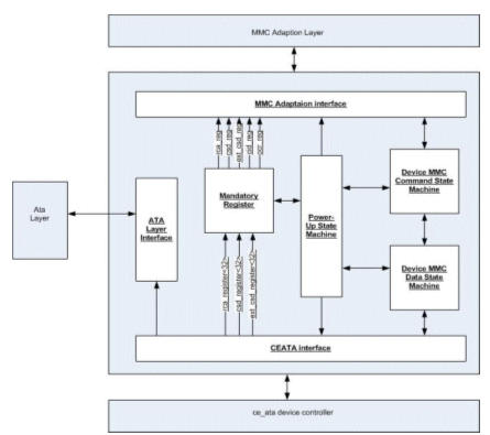
Figure 6 â MMC Layer Module
This module communicates with the ATA layer module, the MMC adapter module, and the CE-ATA controller module. MMC Layer is divided into sub-modules; Mandatory registers, Command decoder, Response logic, Power up state machine, MMC command state machine, MMC data state machine, ATA layer interface, MMC adapter layer interface, and CE-ATA controller interface.
ATA LAYER MODULE
This module communicates with the MMC layer on one side, and the control/status register section of the CE-ATA controller on the other side. The ATA taskfile is implemented in this module. Any other data for reception or transmission come through the CE-ATA Controller FIFOs and directly passed to the write, read FIFOs in the MMC adapter layer module.
The ATA layer module implements the device state machine as specified in CE-ATA specification, and a command decoder. Figure 7 depicts the ATA layer module block diagram with (ata_sm); ATA state machine and (ata_decoder); ATA command decoder submodules and interfaces to the MMC adapter and the CE-ATA controller module.
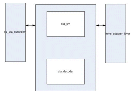
Figure 7 â ATA Layer Module
CE-ATA CONTROLLER MODULE
This module implements a top-level state machine, which will communicate with other modules on the flow of data, and response. This module also implement a RD/WR buffer which is used for data storage to move data either from the ATA layer to the MMC adaptation layer or from the MMC adaptation layer to the ATA layer. The configuration & status registers are also implemented in this module. The next subsections outline this set of sub-modules.
CONFIGURATION AND STATUS REGISTERS
The configuration and status registers will be accessible to a host CPU through an AHB slave interface. All the status bits coming from the different modules, which are running on the MMC clock, will be synchronized before being registered in the register set. Similarly, any configuration bits going from the CEATA controller module will be synchronized to the MMC clock before using them in these modules.
RD/WR BUFFER
The RD/WR buffer is implemented as FIFO in this module. The threshold level of the FIFO is programmable through the configuration registers.
CEATA STATE MACHINE
This module implements a state machine, which is used to control the flow through the CE-ATA device controller. It interfaces to all the modules in the core architecture.
DMA CONTROLLER MODULE
One DMA channel is provided for transmitting, and receiving data to/from external data source to CE-ATA device controller internal buffer. DMA channel efficiently handles all the bulk data transfers. DMA controller with AHB interface comprises the DMA channel interface. DMA channel has descriptors for scatter-gather operations. Figure 8 depicts the DMA controller module block diagram.
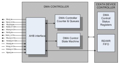
Figure 8 â DMA Interface Module block diagram
AMBA AHB master interface is the core interface between DMA controller and other targets. AHB interface follows AMBA Rev2.0 specifications. DMA controller comprises of controller state machines, address counters and read/write data buffer.
STATUS AND CONTROL REGISTERS
The control and status registers of CE-ATA, and internal coresâ control and status registers are implemented in the CE-ATA device controller core. The AHB slave interface allows access for this set of status and control registers.
CONCLUSION
CE-ATA storage interface standard technology is the state-of-the-art, and optimized SFF storage interface for handheld, portable and consumer electronic devices.
The paper has introduced an introductory overview about the standard technology features. The paper has outlined CE-ATA leverage of existing proven technologies as the proven MMC electrical interface, and the proven ATA command set. The Protocol processing of the basic ATA commands has been outlined in case of interrupts enabled and disabled. The interrupt mechanism, the device initialization and discovery adopted in CE-ATA have been presented.
The paper continues to project
CE-ATA standard protocol in real hardware design cases for host, and device controller IP cores. The hardware design architecture structure of host, and device IP cores is outlined with block diagrams. The main building modules features, functionality and interfaces with other modules have been introduced.
The paper has addressed foundation of a primitive âknow-howâ baseline for the emerging CE-ATA storage interface technology supported by an overview of hardware design cases for CE-ATA host, and device controller IP cores designed for integration into portable, handheld and consumer electronics SOCs.
REFERENCES
1. CE-ATA Organization:
www.ce-ata.org
2. CE-ATA Storage Interface for Handheld Consumer Applicationsâ by Knut Grimsrud & Amber Huffman, Intel Developer Forum, Spring 2005.
http://www.ce-ata.org/docs/SprIDF05_CE-ATA.pdf
3. CompactFlash Association
http://www.compactflash.org/
4. AT Attachment (ATA) Storage Interface:
http://www.t13.org
5. MMCA Association
http://www.mmca.org
6. Storage IP Business Unit, Intellectual Property Division, Mentor Graphics Corporation
http://www.mentor.com/ip
7. AMBA Standard
www.arm.com/products/solutions/AMBAHomePage.html
Related Semiconductor IP
- Specialized Video Processing NPU IP for SR, NR, Demosaic, AI ISP, Object Detection, Semantic Segmentation
- Ultra-Low-Power Temperature/Voltage Monitor
- Multi-channel Ultra Ethernet TSS Transform Engine
- Configurable CPU tailored precisely to your needs
- Ultra high-performance low-power ADC
Related Articles
- Serial ATA and the evolution in data storage technology
- High-Speed PCIe and SSD Development and Challenges
- Integrating VESA DSC and MIPI DSI in a System-on-Chip (SoC): Addressing Design Challenges and Leveraging Arasan IP Portfolio
- How to Elevate RRAM and MRAM Design Experience to the Next Level
Latest Articles
- AutoGNN: End-to-End Hardware-Driven Graph Preprocessing for Enhanced GNN Performance
- LUTstructions: Self-loading FPGA-based Reconfigurable Instructions
- CQ-CiM: Hardware-Aware Embedding Shaping for Robust CiM-Based Retrieval
- GenAI for Systems: Recurring Challenges and Design Principles from Software to Silicon
- Creating a Frequency Plan for a System using a PLL