Can you afford not to have a platform strategy?
As Moore’s law arrives at the 90nm technology node, platform-based design becomes urgent in the SoC area in order to cope with the design and productivity gap. This article shows how OCP fits into the CES Design Services platform concept and how SoC platform development projects benefit from the use of OCP in terms of time-to-market and development cost reductions.
Motivation for platform-based design
Today, there are many factors that make platform-based design a sine qua non . Design has become far too complex to allow designers to start from scratch development and verification at reasonable effort every time. While time-to-market targets have reduced drastically – development from scratch is a thing of the past. Reuse is no longer an option, but a must. And just reusing your own or third party IP modules is no longer enough, reuse as a methodology itself has to be optimized as well. In many cases, it is no longer sufficient to focus on one specific bus protocol because of different applications require very often different bus protocols, for example by a given choice of an embedded CPU. This fact is especially true for design houses like CES Design Services: customer A requires an AMBA bus system, customer B requires an IBM Coreconnect architecture and customer C requires a proprietary module interconnect - cross-domain reuse of existing blocks will be a nightmare. Here the OCP socket definition tries to find a solution: As you know OCP is a socket interface specification that enables comprehensive, standardized definitions of a semiconductor IP core's unique on-chip interfaces. OCP is not a single definition, but instead provides the ability to capture all of a core's signals without imposing limitations on the interaction of the core with a system. Rather than define rigid signal protocols a core must implement, the OCP protocol provides a consistent framework for the identification of all aspects of on-chip data, test and control flows to or from a core. An OCP interface can also be adapted to support new IP core capabilities as a core evolves, without having to resort to a complete re-design of the interface.
Using OCP, intellectual property designers can make their cores independent of specific bus protocols, and hence of any particular design implementation. This allows easier reuse of OCP-compliant cores across multiple SoC designs – a giant step towards cross-application platforms.
The platform concept developed by CES Design Services
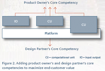
CES Design Services offers customers a tailor-made portfolio of chip development services, from simple subtasks (e.g., design verification) to the outsourcing of concept design, implementation and verification of a complete chip model – whatever customers may need in the given situation. However, all of these outsourced projects or tasks have one thing in common – each partner typically focuses on its core competencies. E.g., for a provider of a safety controller chip for automotive applications it’s important to have the focus on design parts related to the overall system functionality (e.g. the algorithm for crash detection), but it’s not that crucial that he has great expertise in designing the chips maintenance controller or host communication interface. This expertise can be brought in by a design house partner with special expertise in cross-application platforms. Based on this win-win-situation CES has developed its platform strategy.
Customers will receive assistance in everything that, while not falling within their immediate core competence, is still urgently needed to best implement the product’s specific unique selling propositions.
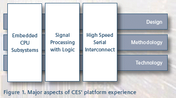
The CES platform concept is based on 3 cornerstones:
- Embedded CPU subsystems:
- Digital signal processing with ASIC/FPGA implementation:
- High speed serial interconnect:

At this point you might ask, what has digital signal processing and high speed serial interconnect to do with platforms. For embedded CPU subsystems this is quite clear – these are classical design platforms, where building blocks are connected to it and the design is done.
When naming the signal processing algorithm a cornerstone of our platform concept, we talk about a so-called methodology platform. You need a solid foundation in algorithm implementation methodology to implement a high level customer algorithm description in a VHDL or Verilog model. Again, each partner has its focus on its core competency: product owner=algorithm design, design house=algorithm implementation.
The third cornerstone of CES’ platform concept is based on a so-called technology platform. Each technology node or device type has it’s own specifics for serial interconnect and you have to deal with them in a very deep technological way.
The CES Design Services platform concept permits customers to focus on their core competencies while assisting them with platforms from a design, methodology and technology point of view. Customer can concentrate on designing the features, that make the product unique and they are enabled to do so rapidly when having a platform strategy and partner in mind.
What role has OCP played so far in CES development projects?
OCP1.0 and OCP2.0 compliant IP modules have been developed within the framework of current CES customer development projects. In the process, CES was able to optimize design risk and efforts as it was possible to use a very clear definition of the OCP standard as a basis for development. On the other hand the use of the proven OCP CoreCreator tool allowed us to speed up the verification setup and furthermore we achieved an improved quality of the verification results. Even in the initial adoption of OCP we gained benefits, because there was no need to invent anything new.

Outlook
CES can look back on a long tradition of memory controller development, from SDRAM controllers to DDR2 memory controllers for ASIC and FPGA implementation. The next step is to port the processor interface of the current DDR2 memory controller IP to be OCP compliant, which should be completed by mid-2005.
About CES Design Services
Located in Vienna, Austria, CES Design Services is a business unit of Siemens Program and System Engineering. CES provides professional services in the area of chip, electronics, and software development for a worldwide range of customers, from startup companies to leading manufacturers. The design services portfolio includes ASIC, FPGA, and SoC design, application software and firmware development, as well as PCB layout, mechanical design, and EDA services.
Related Semiconductor IP
- NPU IP Core for Mobile
- NPU IP Core for Edge
- Specialized Video Processing NPU IP
- HYPERBUS™ Memory Controller
- AV1 Video Encoder IP
Related White Papers
- Case Study: Can you afford to ignore formal analysis?
- It's Not My Fault! How to Run a Better Fault Campaign Using Formal
- Agile Analog's Approach to Analog IP Design and Quality --- Why "Silicon Proven" is NOT What You Think
- How Low Can You Go? Pushing the Limits of Transistors - Deep Low Voltage Enablement of Embedded Memories and Logic Libraries to Achieve Extreme Low Power
Latest White Papers
- Transition Fixes in 3nm Multi-Voltage SoC Design
- CXL Topology-Aware and Expander-Driven Prefetching: Unlocking SSD Performance
- Breaking the Memory Bandwidth Boundary. GDDR7 IP Design Challenges & Solutions
- Automating NoC Design to Tackle Rising SoC Complexity
- Memory Prefetching Evaluation of Scientific Applications on a Modern HPC Arm-Based Processor