The Challenges and Benefits of Analog/Mixed-Signal and RF System Verification above the Transistor Level
Application examples using tools that emphasise graphical capture and exploration.
Andrew K. Betts, Daniel Saias, Hervé Guegan, Nicolas Delorme
Asygn, France
Abstract— Today’s on-chip Analog/Mixed-Signal and RF (A/RF) systems have reached a limit of size and complexity where transistor-level SPICE and FastSPICE simulation approaches cannot deliver a verification solution on time. Challenges include, of course, circuit size, but also the heterogeneous nature of the A/RF systems, their architectural complexity (e.g. modulation schemes, analog/digital mix, in-built configuration, calibration and compensation schemes), and demanding specifications (e.g. high Q, repeated sub-blocks). Such challenges can only be surmounted by moving to a level of abstraction above that of the transistor [Chang]. We consider how this can be done in practice, while maintaining the level of simulation accuracy needed for A/RF verification. The benefits of this approach are illustrated with examples based on new tools that work at the Analog System Implementation (ASI) level of abstraction and which favor schematic, rather than language-based, descriptions of the A/RF system.
I. INTRODUCTION
While tools for analog design are anything but simple, and while progress is constantly being made to improve such tools, the fact remains that they have eluded the levels of automation achieved by their digital counterparts. The master level of description remains the transistor, and for this reason most functional verification efforts are performed at this level of abstraction. Contrast this with standard digital methodologies where signoff functional verification is performed at RTL level, relying on correct-by-construction methodologies to transition to gates, transistors and layout.
However, the increasing size and complexity of on-chip sub-systems makes it impossible to rely only on SPICE simulation for verifying on-chip A/RF systems [Chang]. For example, the following challenges are becoming more prevalent and difficult to tackle:
- Requirement for simulations over many hundreds of clock or carrier cycles in order to verify correct stabilisation or setup of mixed-signal circuits (e.g. PLL setup, real-time configuration, calibration or compensation of circuit parameters).
- Requirement to check the functionality of the complete System On Chip (SOC), taking into account the non-ideal behavior of A/RF sub-systems.
- Requirement for yield analysis involving many process and temperature corners, the number of which has increased massively with the latest technology nodes.
- Need to analyse systems that have very high selectivity (Q) and/or a huge spread in time-constants (e.g. sampled-analog, high ratio of carrier to modulation frequency, ..). These circuit characteristics lengthen simulation runtimes considerably.
- Need for “what if” analysis all the way through the flow, from A/RF system specification through to silicon test (to facilitate debug tasks).
One approach to these issues is to use a FastSpice simulator (e.g. [Takao]). These simulators achieve shorter runtimes than SPICE through automatic simplification of transistor models and, possibly, by partitioning the circuit into sections for which sub-simulations may be run in parallel. The major disadvantages of this approach are (1) the time and trouble required to set the many parameters that control the simulation process, including the degree of transistor model simplification, (2) the stability and accuracy of the final results. In fact, it is possible to obtain FastSpice results that are not only of low precision, but actually false.
A second approach, which seems to becoming popular with SOC teams, is to use a language such as Verilog-AMS or VHDL-A to write behavioral models of A/RF sub-systems [Muhammad][Peralias][Wang]. This method has the considerable merit of raising the abstraction level of simulation above the transistor level, thus reducing simulator runtimes by several orders of magnitude. Drawbacks include the expertise required to write the behavioral models (the languages are powerful, but not trivial to learn, and poor code can lead to unstable models) and the difficulty in ensuring that these models correspond to the implementation being described.
There is no “formal” solution to the latter question at present. Just as we cannot synthesise from higher levels of description down to transistors for analog circuits, so we cannot automatically abstract from the transistor level to higher levels, nor can we do equivalence checking between these levels. In short, there is no generic, automatic solution to these issues in the A/RF domain. It is therefore a question of finding the tools and methods that reduce the probability of human error to an acceptable level.
The tools and method that we describe here work at a level of abstraction that we have called the Analog System Implementation (ASI) level, in order to distinguish it from the higher levels of abstraction that are used, for example, in specification documents and with Matlab [Matlab] and which are strongly equation-based.
In order to fit well with standard practice in A/RF design groups, our preferred tools favor a schematic description of the A/RF sub-systems. Further, control of the tool and exploration of results is possible through use of the graphical interface only. Finally, and most important, these tools use inherently stable algorithms. They are based on models that can be proven stable and, in contrast to FastSpice, automatic model simplification is not used. If instability or lack of convergence is seen in the simulations, then it is due to a property of the circuit, rather than the simulator. Very fast runtimes are therefore achieved without the drawbacks of FastSpice or language-based solutions.
II. FLOWS
The fundamental challenge in ASI-based verification is the implied need to go “bottom-up”. That is, if the verification simulation problem is treated in isolation, with the task defined as “inputs = transistor netlist + vectors + expected results, output = pass/fail”, then we must somehow work out how to get from the transistor level netlist to the ASI description. This observation leads us to two fundamentally different approaches:
- ASI-based verification as an isolated task
- ASI-based verification as part of a flow built to support this verification style
The approach taken will depend upon the project in question, and we do not discount either. While life is generally more comfortable if the second approach can be taken, this implies advanced planning and investment that is not always possible.
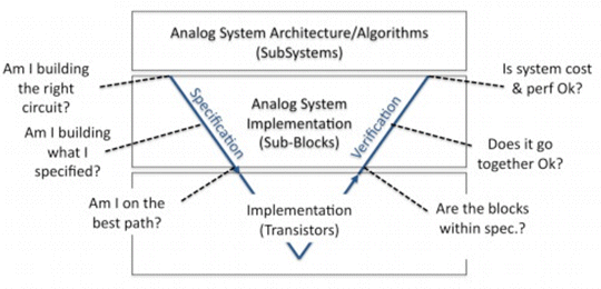
We will give an example of the first approach, which is more ad-hoc than the second, in the next section. The second approach starts at the point where a simulatable specification is established for the A/RF system to be implemented, and this approach is described in [Betts]. In this case, the outcome of the ASI-based verification is much easier to predict, since there is a planned continuity from the work of modeling the intended implementation through implementation and assembly of the component blocks/IPs to final verification of the A/RF subsystem. Since an ASI-level model is available throughout the process, with updates from knowledge gained during implementation gradually refining its accuracy, the process should be a convergent one and the number of last-minute surprises is reduced. The following diagram summarises the process:

III. EXAMPLES AND BENEFITS
Our first example was verified at the ASI level after the designed was actually completed at the transistor-level.
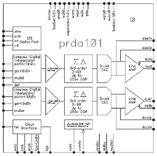
It consists in a stereo audio DAC IP designed for easy IC level integration of audio systems. Combining low power with high dynamic performance, it is naturally intended for portable and/or demanding applications such as MP3 players, PDAs and cellular phones.
It is built around a 32/64/128/256x interpolating digital filter, a 3rd order MASH Sigma Delta modulator and a single stage multi element DAC, followed by a highly linear line buffer amplifier.
The fully differential architecture of the analogue front-end guarantees a strong immunity to any common mode perturbation when integrated in a noisy environment. It is manufactured in ATMEL high-density standard 0.13µm CMOS process thus offering a cost effective solution when integrated in a System on Chip (SoC).
The feature “Click-less” has been added in order to minimize pops and clicks, during the startup/shut-down phases.
The circuit’s block diagram is shown below:

The IP main features are as follows:
- 90dB dynamic range
- 8 to 96kHz sampling frequency
- 10 mW typical consumption @ 3V supply
- Vector quantized dynamic elements matching (DEM) engine
- 120 to 0dB / 1dB step programmable attenuation
- De-emphasis filter
The cell dimensions are 1mm2 for the analog part and 0.4mm2 for the digital part, representing 46Kgates, reduced to about 1Kgate for simulations of the A/MS part of the IP.
As this example falls into the first category mentioned before, some translation work had to be carried out to produce de ASI-level models from the transistor-level netlist. Analog transistor-level cells (e.g. opamps, switches, references…) and digital transistor-level gates were mapped to a set of analog and digital ASI primitives. Thanks to the highly hierarchical nature of the design, the overall manual conversion effort was roughly one man-day. This effort is rewarded by far when it comes to perform the verification simulations, as shown in the table below.
| Simulation engine | Abstraction level | CPU Time |
| Spice | Transistor | 80 hours |
| Spice | ASI (VerilogA macromodels) | 10 hours |
| Asygn tools (www.asygn.com) | ASI (Asygn primitives) | 2 minutes |
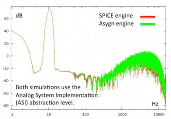
With the same abstraction level (i.e. macromodels), the ASI simulation running on a tool designed specifically for this level of abstraction provides a x300 improvement in terms of CPU time, while maintaining the same level of accuracy: the following figure shows how close the simulation results remain (the two plots are almost indistinguishable in B&W!).

The conclusions of this first example are:
- A great deal of verification coverage can be achieved at very modest investment, even when ASI-based verification has not been planned from the start in the global design flow.
- Simply moving to the ASI level of abstraction will provide limited gains if the simulator used is not optimised for operation at the level of abstraction. Specifally, a SPICE-type simulation engine, even when used with ASI-level macromodels, will run much slower than a purpose-built ASI-level simulator.
Our second example is one of a system for which ASI-level verification was planned from the beginning .
The Analog/Mixed-Signal (AMS – a subset of A/RF) system in question is an imaging array. Several hundreds of thousands of pixels, including their non-ideal characteristics, must be simulated. The verification objectives are:
- To ensure that the array is functionally correct.
- To ensure that the system meets specification in the presence of different non-ideal effects, some of which are unevenly or randomly spread across the pixel array.
- To be able to rapidly and visually debug any errors found.
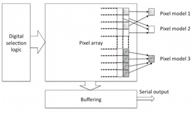
This example is a good illustration of the difficulty in adapting generic tools to specific A/RF systems. In this case, the huge array of pixels is a major challenge to any analog simulator. This was overcome by adapting and reconfiguring components from generic tools into a custom setup. In particular, the pixels in the array were modeled at the ASI level and then compacted, for faster simulation. Further, the simplicity of the pixel models (when compared to frequently encountered analog components such as amplifiers, oscillators, etc) gives us the opportunity to provide an automatic extraction of the ASI model parameters from SPICE results, thus overcoming one of the major obstacles in ASI-based verification. This approach allows the final system to attain “signoff” status in the sense that regression runs may be automatically run at ASI level using as input SPICE netlists extracted from layout – without any manual intervention.
A sketch of the system is provided below:

The verification system is currently functional and we are in the process of refining the overall specification-to-tapeout flow. The runtime improvements obtained through this ASI-based, custom approach are very considerable, allowing us to investigate many types of non-ideal phenomena that were previously out of bounds to simulations. In the past, even the simulation of ideal behavior was infeasible on the full imaging array.
IV. TOOL REQUIREMENTS
Our experience from the verification projects described above, plus many others in the A/RF and digital domains (and even in micromechanical systems) has led us to the following wish list for supporting tools:
- Tools need to be as integrated as possible into standard A/RF designer environments. This is not simply a matter of habit and comfort, but also to avoid double-entry of information and to minimise the probability of human error in general.
- A corollary to the preceding point is that schematic entry must be used wherever possible, since this is the preferred way of capturing circuits of most A/RF designers (as opposed to writing descriptions using a circuit description language) .
- In addition to standard batch-style inputs and outputs, tools need to provide a high level of interactivity, allowing users to perform dynamic “what-if” type analyses. This type of functionality is more commonly associated with specification and design, but we have found that it is also essential for debug, which represents a large proportion of engineering time spent in verification. Again, if these interactivity features can be presented graphically, so much the better.
- A critical aspect of the interactive debug activity, just mentioned, is understanding the relationship between signal outputs from the circuits under test and the contributing components (wanted and less welcome) of these signals. It is important that verification tools allow the breakdown of output signals into such components.
- Since it is not (yet) possible to automatically abstract from the transistor to the ASI level, an extremely important common reference between the two levels of abstraction is the testbench. Tools for ASI-level verification must therefore assist designers to maintain consistent testbenches between the ASI and transistor levels.
V. CONCLUSION
Progress in chip technology and Analog/Mixed-Signal and RF (A/RF) systems design makes it imperative to develop verification methodologies and tools that exploit the Analog System Implementation (ASI) level of abstraction (i.e. we must move above the transistor level). There is no generic method or tool that can help this process in all cases. Sometimes it is not even possible to plan a complete specification-to-silicon flow incorporating ASI-level verification, and we have to anticipate these circumstances also. Examples have been given of both planned and less planned projects incorporating ASI-level verification, illustrating the use of new tools that are well adapted to this task. Based on this experience we list a number of features (some of which are already implemented in our tools, others of which are in development) that facilitate ASI-level verification of A/RF systems.
REFERENCES
[Betts] Betts; Delorme; Making the most of the system level in analog design; EETimes; 28 June 2010; http://www.eetimes.com/design/eda-design/4200967/Making-the-most-of-the-system-level-in-analog-design
[Chang] Chang, H.; Kundert, K.; Verification of Complex Analog and RF IC Designs; IEEE Proceeding; March 2007; http://ieeexplore.ieee.org/xpl/freeabs_all.jsp?arnumber=4167767 or http://www.designers-guide.com/docs/proc2006.pdf
[Matlab] MathWorks - MATLAB and Simulink for Technical Computing; http://www.mathworks.com
[Muhammad] Muhammad, K. et al;Verification of RF SoCs: RF, analog, baseband and software; http://ieeexplore.ieee.org/xpl/freeabs_all.jsp?arnumber=1651166
[Peralías] Peralías, E.; A VHDL-based Methodology for the Design and Verification of Pipeline A/D Converters; DATE 2000 Conference; http://www.date-conference.com/proceedings/PAPERS/2000/DATE00/PDFFILES/07D_1.PDF
[Takao] Takao Ito; Analog behavioral models reduce mixed-signal LSI verification time; EETimes; 22 June 2007; http://www.eetimes.com/design/industrial-control/4009956/Analog-behavioral-models-reduce-mixed-signal-LSI-verification-time
[Wang| Wang et al; Event Driven Analog Modeling for the Verification of PLL Frequency Synthesisors; BMAS 2009; http://www.bmas-conf.org/2009/2-1_Paper.pdf
Related Semiconductor IP
- ReRAM NVM in DB HiTek 130nm BCD
- UFS 5.0 Host Controller IP
- PDM Receiver/PDM-to-PCM Converter
- Voltage and Temperature Sensor with integrated ADC - GlobalFoundries® 22FDX®
- 8MHz / 40MHz Pierce Oscillator - X-FAB XT018-0.18µm
Related Articles
- Transactional level as the new design and verification abstraction above RTL
- Accurate System Level Power Estimation through Fast Gate-Level Power Characterization
- EDA focus shifts to system level design
- VMM based multi-layer framework for system level verification
Latest Articles
- An FPGA-Based SoC Architecture with a RISC-V Controller for Energy-Efficient Temporal-Coding Spiking Neural Networks
- Enabling RISC-V Vector Code Generation in MLIR through Custom xDSL Lowerings
- A Scalable Open-Source QEC System with Sub-Microsecond Decoding-Feedback Latency
- SNAP-V: A RISC-V SoC with Configurable Neuromorphic Acceleration for Small-Scale Spiking Neural Networks
- An FPGA Implementation of Displacement Vector Search for Intra Pattern Copy in JPEG XS