Agile Design for Hardware, Part II
David Patterson and Borivoje Nikolić, UC Berkeley
EETimes (7/30/2015 07:00 AM EDT)
In the second of a three-part series, two Berkeley professors suggest its time to apply Agile design techniques to hardware.
We asked readers of Part I to guess the cost of a prototype run of 28 nm chips, as Agile development relies on a sequence of interim prototypes versus the One Big Tapeout of the traditional Waterfall process. Here are the results:
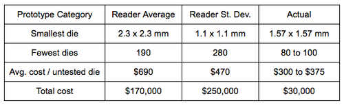
The surprisingly low manufacturing cost of prototype chips—one fifth the readers’ estimate—means Agile development is eminently affordable, even for academics. (See www.AgileSoC.com for more evidence.) It also calls into question the current high cost of designing SoCs using the Waterfall process. Having established Agile’s viability, based on our experience we propose four guidelines to lower development costs.
To read the full article, click here
Related Semiconductor IP
- NPU IP Core for Mobile
- NPU IP Core for Edge
- Specialized Video Processing NPU IP
- HYPERBUS™ Memory Controller
- AV1 Video Encoder IP
Related White Papers
- Agile Design for Hardware, Part I
- How to design secure SoCs, Part II: Key Management
- How to design secure SoCs, Part III: Secure Boot
- Integrating analog video interface IP into SoCs delivers superb image quality (Part II)
Latest White Papers
- Transition Fixes in 3nm Multi-Voltage SoC Design
- CXL Topology-Aware and Expander-Driven Prefetching: Unlocking SSD Performance
- Breaking the Memory Bandwidth Boundary. GDDR7 IP Design Challenges & Solutions
- Automating NoC Design to Tackle Rising SoC Complexity
- Memory Prefetching Evaluation of Scientific Applications on a Modern HPC Arm-Based Processor