A powerful dual-mode IP core for 802.11a/b Wireless LANs
by Michel Eftimakis, NewLogic
Sophia Antipolis, France
Abstract
This paper presents the WiLD (WLAN IP for LSI Designs), a powerful dual-mode IP core and the associated software stack for 802.11a/b Wireless LANs. It starts by a short introduction to WLAN systems to understand the global context of the project. Then, the architecture of the WiLD core and platform is presented, highlighting its original structure and displaying its performance.
The IP integration in a system and the design methodology are then developed, explaining the constraints that may emerge during the creation of an ASIC. Finally, the conclusion will show the potential applications for the WiLD products and their future evolution.
Introduction
WLAN systems
More and more Wireless Local Area Network (WLAN) systems are being installed these days, and the number of users is increasing at a very high rate. Being able to connect a computer to a network without having to physically connect a wire to a plug is very convenient: it reduces the cost of wiring offices, helps sharing high-speed internet connections at home, allows customers to surf the web in cafés, removes the need of a physical reconfiguration in case of a computer move, and has numerous other advantages…
However, an increasing number of companies are thinking of new ways to use the WLAN connections in innovative products, e.g. in wireless portable flat-screen TV sets that you can move around in the home without needing a wire connection to the receiver, or digital camcorders that connect to a PC with a wireless link.
To address the need of a unified standard that would allow multiple devices to interoperate, several organizations have created WLAN standards. The most popular to date is the 802.11 standard, written by the IEEE. This standard belongs to the 802 family of standards that allow easy bridging between several different means of transporting information over different media. Each different medium is addressed by a different standard, containing different physical and medium access layers, e.g. the well-known 802.3 standard (Ethernet).
The 802.11 standard [1] supports several physical layers, the most popular being DSSS/CCK in the 2.4 GHz ISM band (called 802.11b [2]) and OFDM in the 5 GHz band (802.11a [3]). More layers are still being developed (like 802.11g).
There are many different ways to implement the WLAN functionality into a product. This mainly depends on the product: if it is flexible enough, it may be possible to use one of its existing ports to plug-in an expansion card. If the device belongs to an existing family of products, a new generation may come with built-in WLAN capability, or a new high-end appliance may propose this feature at a premium price. New products are also built from scratch, and may be centered on the WLAN capability. In the last two cases, an internal solution (i.e. motherboard) is preferred, to reduce the cost of the implementation.
WiLD
The WiLD system addresses the needs of the chip or application manufacturers who want to integrate the 802.11 WLAN functionality in their product. It contains all the parts that are necessary to make the system run, so that the customers can concentrate on the final application and only have to integrate the IP in their ASIC.
The WiLD product family is composed of several elements designed to function together in an optimal way:
- WiLD RF – dual-band (2.4 GHz / 5 GHz) CMOS radio IP
- WiLD Software – multi-standard (802.11a / b / e / g / h / i…) protocol software
- WiLD MAC – a powerful processor-based hardware platform
- WiLD Modems – hardware signal processing blocks dedicated to a given modulation scheme (e.g. the 802.11a and 802.11b modems are different)
Following NewLogic commercial strategy, these products are only available as IP, while the company proposes design services to integrate the IP into complete SoC. The radio IP is only available in hard layout format for TSMC, and would need to be ported to another technology if required. The other hardware IP is delivered in synthesizable RTL code that can be tuned to the needs of the users.
This paper will mostly focus on the MAC and Modems part.
The architecture
Architecture of the WiLD Platform
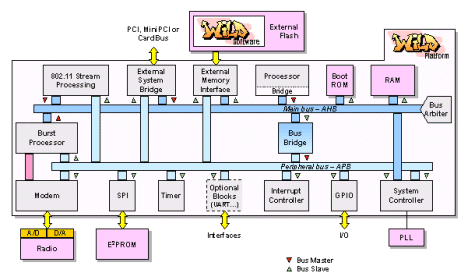
The WiLD MAC platform is presented below. It is centered on an AHB/APB bus system [5], allowing it to be very flexible, as a lot of peripherals are available for these busses. The processor is typically an ARM7TDMI, but any equivalent or more powerful processor would also fit in the system.
A general view of the block diagram is that data is exchanged with the radio on one side, while it flows to and from a host on the other side, via the External System Bridge (see diagram).
The platform has been designed to be usable for many different projects and is not specific to 802.11 or any wireless standard. It has a high bandwidth of 320 MB/s at 80 MHz; well over the 54 Mb/s requirement for 802.11a. The backbone bus is used to move data between the processing blocks, and the processor uses the remaining available bandwidth for fetching the code and data.


Direct memory access is built in all data processing blocks so that the processor is not involved in moving blocks of data: it can just concentrate on handling the protocol. This ensures that a low performance processor can handle very high data rates, and that the required processing power does not grow linearly with the data rate.
This complete platform can be integrated into more complex systems, with a suitable bridge. This makes it a closed subsystem, where it is possible to ensure that the required performance targets are met. This is especially important in 802.11 devices, because a software implementation is necessary to keep the system open to standard upgrades and extensions while very fast response times are required to respond to certain events. The processing times must therefore be tightly controlled and it is essential to avoid interference from the external host.
The internal RAM of the platform is used to store the software and to buffer the data packets. This allows downloading the firmware from an external flash or directly from the host, making a product field-upgradeable. An external RAM can also be used to augment the buffering capacity in particularly demanding applications.
The External System Bridge is the only interface to the controlling system. In the case of a chip built for a PC expansion card, this would be a PCI, MiniPCI or CardBus interface. It is also possible to integrate the WiLD Platform inside an SoC, where it is more efficient to use another bridging mechanism, e.g. a dual-port RAM or a simple bus-to-bus bridge.
Architecture of the 802.11 specific blocks
All the data flow processing required to support the 802.11 standard is handled by specific blocks integrated in the WiLD Platform.
The sample stream coming from the radio in reception mode is first handled by the modem, which performs all required signal processing: filtering, compensation of DC offset & I/Q mismatch, timing & frequency synchronization, estimation & compensation of the channel response and finally demodulation & detection of the data symbols.
Then a burst processor takes care of the data packets, packet and frame timings and data streaming. It also helps the software to meet the tight timing constraints and to manage the traffic priorities for QoS handling.
The data portion is forwarded to the stream processing block, that performs decryption, CRC computation and checking, and FEC decoding. This block is able to handle different algorithms: the original RC4 / WEP encryption, well known for having been cracked and therefore not secure (but needed for backward compatibility) and the new Advanced Encryption Standard (AES) algorithm that is required for the 802.11i security extension.
The transmission mode of course uses the inverse data path.
The most sensitive part of the design is of course the signal processing part, since it determines the performances of the final system in terms of packet or bit error rate (PER or BER). It has been subject to intensive algorithm simulation and research.
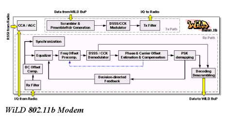
A block diagram of the WiLD 802.11b Modem is presented below, showing the main blocks and the selected architecture. The transmission path, in the top part, is well defined in the standard, except for the Tx filter. The reception path, however, is completely left to the designer and no guidance is given in the standard.
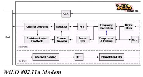
The WiLD 802.11a Modem shown below is similar in principle: the Tx path is well defined in the specification and the Rx path is the portion that differentiates the implementations. The way it is designed has a dramatic impact on the final performance.


Performances
The performance of the reception directly impacts the behavior of the WLAN device in a real RF environment. Multiple reflections of the radio waves create interference that is compensated by the equalizer, while the other blocks compensate for various other effects and finally demodulate the data symbols. The ETSI and IEEE have defined statistical channel models in various environments that are used to simulate this effect.
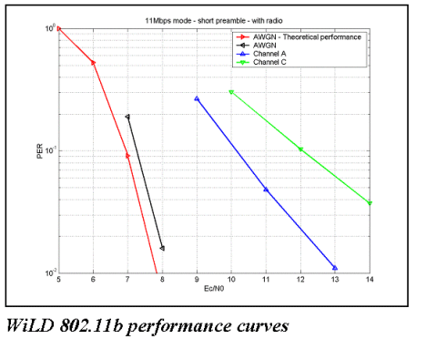
To assess the quality of the implementation, the performance is shown as curves that display the PER as a function of the signal to noise ratio EC/N0 (Signal Energy per chip over Noise Power Spectral Density), given in dB. The higher signal to noise ratio, the better the quality of the received signal.
An example of such a performance curve is shown below, for the IEEE 802.11b standard. The curve on the left shows the theoretical performance of an 802.11b system in a very simple noisy environment (AWGN – Additive White Gaussian Noise channel). This is the performance bound that can only be attained by an ideal receiver.
The three curves on the right are the performances of the WiLD 802.11b modem in different radio environments, taking the radio impairments effects (I/Q mismatch, various offsets…) into account. The performance in AWGN (second from the left) shows the quality of the baseband implementation and the ability of the modem to compensate for the radio effects.
The other two curves (on the right) plot the PER vs. signal to noise ratio in some of the multipath channels defined by the ETSI (European Telecommunications Standards Institute). These channels simulate small and large office environments and are used to assess the quality of the equalizer.

For a given signal-processing algorithm, the quality of the modem implementation is linked to the size of the data paths in each processing steps. The choice of a given word length is the result of long hours of simulation to trade off gate count vs. implementation quality.
IP development & integration
Design methodology & flow
In order to develop such a complex system, a complete team comprising experts in many different domains had to be put in place. First, as highlighted in the previous part, a System team has worked on the signal processing algorithms and their implementation in the circuit. Architecture designers in the System team also determined the architecture of the system, along with software and RF system engineers.
The Hardware development group then was in charge of the IP development. It contained digital designers, RF/Analog designers and backend engineers but also board designers to build FPGA prototypes.
The Software team is divided in real-time software designers, protocol software designers and application software designers to handle all the different parts of the implementation.
The first steps in the design process are the system study and the prototyping platform definition. After a draft of the complete system has been defined, the partitioning and interfaces between the main parts (RF, Baseband hardware, Software) are outlined and the system/architecture engineers can detail the specifications of all different blocks.
The designers then proceed in the implementation of the blocks, using RF/analog, VHDL and SDL (protocol description language used in software) simulation tools to verify the design. The testbenches used in this verification phase are refined with the results obtained by the other teams, e.g. the SW behavior is modeled in the HW simulation, or the RF performances are fed back to the modem testbench. This cross checking is necessary to ensure that no divergence occurs during the design flow, which would lead to a fatal problem when the final product is released.
Then the prototyping phase takes place. The RF prototype must be a test chip, since there is no other way to ensure that a radio frequency system works, but the hardware can be prototyped on an FPGA board. This methodology, already highlighted and described in many places (e.g. [4]), is an extremely efficient way to quickly debug a complex system.

As the requirements for the WiLD project were very high in terms of gate count, compared to existing prototyping platforms, a new board has been designed especially for this purpose. It hosts two high-end FPGA that are specified as 6 million FPGA-gates each. This allows the prototyping of between 500 and 600 kGates in each FPGA (“real” ASIC NAND2-equivalent gates).
The board, called WiLD Card, is depicted above. It also features several connectors, to allow plugging it into PCI and CardBus slots, and a digital port that can be used for a variety of applications, ranging from a direct wire link to another WiLD Card, to the connection of a radio daughter board. Test ports are also available to monitor the internal activity and debug the circuit.
This board has been used to validate the WiLD IP, and verify that the dual-mode 802.11a/b is working correctly with the complete protocol stack, in a realistic environment. This gave us a high confidence in the quality of the developed IP, and allowed in-depth verification that would not have been possible with simulation only.
The IP development work is completed by the IP packaging. This step consists in collecting all the parts necessary to the customers for the IP integration, preparing training and creating a complete set of files containing code, documentation, scripts, special tools, examples, design files… This is the productization phase of the IP, which is now ready for integration into ASICs.
Complete WLAN system development
To build a system on top of WLAN IP, after having selected and licensed all the required parts, a company needs to follow a complete flow. This could be very short in certain cases, e.g. when the ASIC only contains the WLAN IP, or it can be a relatively longer process when the IP needs to be integrated into a more complex SoC.
To simplify the integration work, customers can reuse the prototyping platform to build a realistic trial product and interface it with other devices, which may also be other prototyping platforms. Building around the existing FPGA board allows to directly start on the development or adaptation of the final software application, without having to wait for the samples of the final ASIC.
The hardware integration process can then run in parallel, and it benefits from the fact that the IP has been proved separately. There is therefore only the need for verification of the interfaces, and no significant amount of time has to be spent on verification of the WLAN protocol itself. The designers thus can concentrate solely on the final application.
Conclusion
We have seen that the design of high-end WLAN systems challenges the methodology that was put in place for earlier designs, but that the prototyping platform strategy was still very helpful in the development flow. As standards and products are becoming more and more complex, highly skilled people are needed in the development teams, with very different backgrounds and domains of expertise. This prevents many companies from building themselves the necessary parts to implement the standards, and strongly pushes towards IP licensing from an expert company.
Moreover, as time to market becomes still more important, the product manufacturers have less time to spend in R&D, and benefit largely from acquiring external IP since it allows quick low-risk development of a working product. It is clearly not sensible anymore to build million-gate designs from scratch.
The trends in WLAN are towards more integration, with everyone talking about the famous “single chip solution”. NewLogic is definitely pushing in that direction, with a complete set of products – from RF to application software – that can be integrated into standard CMOS chips. The integration of several standards into the same chip is also supported by the WiLD IP, since several modems are available: 802.11a, 802.11b, to be followed by 802.11g and other evolutions of the standards. This will ultimately result in single chips supporting multiple standards and customer logic, allowing extremely integrated products mass-produced at a ridiculously low cost.
References
[2] “Wireless LAN Medium Access Control (MAC) and Physical Layer (PHY) specifications: Higher-speed Physical Layer Extension in the 2.4 GHz Band”, IEEE Standard 802.11b, September 16th, 1999
[3] “Wireless LAN Medium Access Control (MAC) and Physical Layer (PHY) specifications: High-speed Physical Layer in the 5 GHz Band”, IEEE Standard 802.11a, September 16th, 1999
[4] Michel Eftimakis, “Optimized development of a Bluetooth™ system”, SAME 2000 conference, October 25th, 2000
[5] ARM, “AMBA specification v2.0”, Ref: IHI 0011A, May 13th, 1999
Glossary
An overview of the cited 802.11 standards:
- 802.11 – Original WLAN system based on DSSS modulation in the 2.4 GHz ISM band, running at 1 or 2 Mb/s.
- 802.11a – OFDM modulation in the 5 GHz band, running at 6, 9, 12, 18, 24, 36, 48 or 54 Mb/s.
- 802.11b – DSSS/CCK modulation in the 2.4 GHz band, running at 1, 2, 5.5 or 11 Mb/s.
- 802.11e – Quality of Service (QoS) extension, using FEC (Forward Error Correction), useful for multimedia applications. Still in draft state.
- 802.11g – Mix of DSSS, CCK and OFDM modulations in the 2.4 GHz band, combination of .11a and .11b packets in a single band. Still in draft state.
- 802.11h – Transmit Power Control and Dynamic Frequency Selection extensions, necessary to be compliant with European regulations. Still in draft state.
- 802.11i – Security enhancement extension, using the Advanced Encryption Standard (AES) algorithm defined by the National Institute of Standards and Technology (NIST) to replace DES. Still in draft state.
Related Semiconductor IP
- 8MHz / 40MHz Pierce Oscillator - X-FAB XT018-0.18µm
- UCIe RX Interface
- Very Low Latency BCH Codec
- 5G-NTN Modem IP for Satellite User Terminals
- 400G UDP/IP Hardware Protocol Stack
Related Articles
- Interstellar: Fully Partitioned and Efficient Security Monitoring Hardware Near a Processor Core for Protecting Systems against Attacks on Privileged Software
- CAST Provides a Functional Safety RISC-V Processor IP for Microchip FPGAs
- Design and implementation of a hardened cryptographic coprocessor for a RISC-V 128-bit core
- Customizing a Large Language Model for VHDL Design of High-Performance Microprocessors
Latest Articles
- SNAP-V: A RISC-V SoC with Configurable Neuromorphic Acceleration for Small-Scale Spiking Neural Networks
- An FPGA Implementation of Displacement Vector Search for Intra Pattern Copy in JPEG XS
- A Persistent-State Dataflow Accelerator for Memory-Bound Linear Attention Decode on FPGA
- VMXDOTP: A RISC-V Vector ISA Extension for Efficient Microscaling (MX) Format Acceleration
- PDF: PUF-based DNN Fingerprinting for Knowledge Distillation Traceability