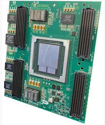
PRO DESIGN Launches New proFPGA XCVU37P FPGA Module for Prototyping and Verification of High Bandwidth Memory Designs
MUNICH -- February 27, 2020 -- PRO DESIGN, leading supplier of FPGA based prototyping systems, today launched its new proFPGA XCVU37P FPGA module for its flexible proFPGA product family. This new FPGA module, assembled with a Xilinx® Virtex® UltraScale+™ XCVU37P FPGA including High Bandwidth Memory (HBM), addresses ASIC designers who need an extremely efficient and best-performing FPGA-based prototyping solution for AI, Deep Learning, Data Centre, image/video analysis and other bandwidth-intensive applications.
In many of today’s applications highest compute power is required and together with this also a massive increase in memory bandwidth is mandatory where traditional SDRM technology has long since reached its limit. Therefore, other solutions are required, solutions like Xilinx’s high bandwidth memory (HBM) FPGAs which provide tremendous memory bandwidth compared to their traditional counterparts.
With proFPGA prototyping systems normally required memories like DDR4, LPDDR4 or QDR will be plugged via extension boards on the FPGA modules and will be connected to the user design inside the FPGA. For HBM this isn’t possible anymore, because HBM isn’t available as dedicated parts that can be soldered on a board. For the HBM in the Xilinx® Virtex® UltraScale+™ XCVU37P FPGA, a silicon stacking technologies is used where FPGA fabric and DRAM are placed next to each other in the same package. This method offers significant improvements in performance and latency compared to external chips that are soldered on PCBs and where you may even have connectors or sockets in between memory and FPGA.
proFPGA customers can also benefit and use HBM in their FPGA-based prototyping setting since the new proFPGA XCVU37P HBM FPGA module is fully integrated in the proFPGA system environment.
The new proFPGA XCVU37P HBM FPGA module is designed and optimized for best signal integrity and maximum performance. In combination with high-end PCB material and high-speed connectors, the new FPGA module reaches an outstanding point-to-point speed of more than 1.4 Gbps single-ended over regular FPGA IOs and a performance of up to 25 Gbps over the multi-gigabit transceivers (GTY).

proFPGA VU37P HBM FPGA Module
The innovative FPGA module, which is assembled with the latest Xilinx® Virtex® UltraScale+™ XCVU37P FPGA contains 8 GB High Bandwidth Memory (HBM) DRAM and offers an ASIC equivalent capacity up to 15 million gates. Further, the module offers on 4 extension sites 519 free accessible user I/Os and 72 multi-gigabit transceivers.
“The memory bandwidth requirements from a lot of our customer’s applications like AI, Machine Learning or Data Centre are increasing exponentially and these are very difficult and quite challenging to verify with traditional methods. Customers asked us to solve this verification issue and we are more than happy, that we can present a solution with our new proFPGA XCVU37P HBM FPGA module from which many of our customers who had applications with memory bottlenecks can benefit from. They now have a FPGA module, which can be easily integrated in the proFPGA environment and which gives them the possibility to have full access to the HBM technology in their FPGA prototype.” said Gunnar Scholl, CEO from PRO DESIGN.
The new proFPGA XCVU37P FPGA Module can be easily assembled on the proFPGA uno, duo and quad motherboards and can also be combined with other proFPGA FPGA modules. It is fully compatible with all proFPGA accessories like interface boards and interconnection cables.
Availability
The proFPGA XCVU37P FPGA module will be available at beginning of March 2020.
Demonstration
PRO DESIGN will demonstrate the proFPGA XCVU37P FPGA module at DVCon US, in San Jose, CA at booth #505 on March 2-4, 2020
For more information please visit: https://dvcon.org/
About proFPGA
The proFPGA product family is a complete, scalable, and modular multi-FPGA prototyping solution, which fulfills the highest needs in the areas of ASIC and IP Prototyping and pre-silicon software development.
About PRO DESIGN
The privately-held company was founded in 1982 and has about 100 employees at various facilities in Germany, France, and the US. PRO DESIGN has more than 37 years of experience in the EDA market, and as a provider in the E²MS market.
For more information, please visit: http://www.proFPGA.com
Related Semiconductor IP
- SHA-256 Secure Hash Algorithm IP Core
- EdDSA Curve25519 signature generation engine
- DeWarp IP
- 6-bit, 12 GSPS Flash ADC - GlobalFoundries 22nm
- LunaNet AFS LDPC Encoder and Decoder IP Core
Related News
- PRO DESIGN Extends FPGA Based Prototyping Portfolio With proFPGA XCVU13P Module - Offering Highest Interface and System Performance
- PRO DESIGN Unveils Affordable Virtex 7 Based FPGA Module for Multi FPGA Prototyping
- PRO DESIGN Releases FMC Adapter Kit for Its proFPGA Virtex 7 Based FPGA/ASIC Prototyping Solution
- PRO DESIGN Completes FPGA based Prototyping Portfolio with proFPGA Uno V7 System
Latest News
- Rebellions Collaborates with SK Telecom and Arm Targeting Sovereign AI and Telecom Infrastructure
- Sarcina Launches UCIe-A/S Packaging IP to Accelerate Chiplet Architectures
- BrainChip Unveils Radar Reference Platform to Bridge the ‘Identification Gap’ in Edge AI
- Siemens accelerates AI chip verification to trillion‑cycle scale with NVIDIA technology
- SiFive Raises $400 Million to Accelerate High-Performance RISC-V Data Center Solutions; Company Valuation Now Stands at $3.65 Billion