Government of India creating enabling environment for Semiconductor Design Community with direct access to National Chip Design Infrastructure
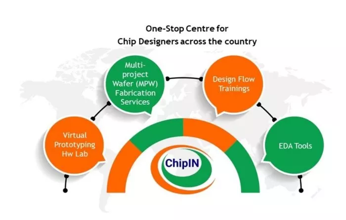
November 27, 2024 -- ChipIN Centre, one of the largest facilities established at C-DAC, offers an extensive range of semiconductor design workflows and solutions, striving to bring national chip design infrastructure directly to the semiconductor design community across the country. It is a centralized facility which hosts the most advanced tools for the entire chip design cycle (going up to 5 nm or advanced node).
It also offers compute and hardware infrastructure, IP cores, and expertise to provide comprehensive services for design fabrication at the SCL foundry and packaging to academic institutions under C2S (Chips to Start-up) Programme and DLI (Design Linked Incentive) Scheme of Ministry of Electronics and IT, Government of India.

Charkha to Chips: Atmanirbhar Bharat
Presently engaged with an estimated number of 20,000+ students at 250+ academic institutions and entrepreneurs at 45 start-up projects, ChipIN Centre aims to provide access of state-of-the-art EDA (electronic design automation) tools to 85,000 students at B.Tech, M.Tech and PhD level to design semiconductor chips within 5 years to meet the objectives of Atmanirbhar Bharat. List of institutions getting access of EDA Tools is at https://c2s.gov.in/EDA_Tool_Support.jsp

Considering the growing demand for EDA tools from Siemens amongst researcher & opportunity to scale the established infrastructure at ChipIN Centre, Siemens has extended the current usage scope of its EDA tools from 120 colleges to 250+ colleges under Chips to Start-up (C2S) Programme and latest powerful Veloce™ hardware-assisted verification solution from Siemens, to the companies approved under the DLI Scheme.
Veloce to address SoC and IC Design challenges
Veloce from Siemens comprising of the following main components – Veloce Strato hardware & OS, Veloce Apps and Veloce Protocol Solutions, has a compute facility of 128 CPU cores and capacity of 640 million gates. This addresses the verification and validation challenges faced by designers of complex SoCs (system on a chips) & highly sophisticated IC (integrated circuit) designs. Details can be seen at https://vegaprocessors.in/hep.php

ChipIN centre to boost India's Semiconductor Vision
“We were receiving the huge demand from students, researchers, faculty members & entrepreneurs across the country in respect of further enhancing & extending the EDA & design solutions from Siemens to more organizations. The enhanced support from Siemens at the ChipIN Centre will play a crucial role in fulfilling the vision of turning India into a semiconductor powerhouse.” said Ms. Sunita Verma, Group Coordinator (R&D in Electronics & IT), Ministry of Electronics and IT.
Empowering next gen for a Self-Sustaining Semiconductor Ecosystem
“India today presents a significant opportunity for aspiring entrepreneurs and researchers to be at the forefront of designing and redefining the semiconductor systems, devices and products of the future. Siemens is proud to extend its participation in the “Chips to Start-up (C2S) Programme” of Government of India and MeitY by expanding access of its state-of-the-art EDA technology solutions to 250 educational institutions across India. Our contribution is a testament of alignment with the nation's unwavering commitment to building a robust and self-sustaining semiconductor ecosystem by empowering the next generation of engineers, researchers and entrepreneurs to drive India's technological advancements and propel the nation towards becoming a global powerhouse.” – Ruchir Dixit, Vice President & Country Manager, EDA, Siemens Digital Industries Software.
Related Semiconductor IP
- 16-Bit xSPI PSRAM PHY
- ASIL B Compliant MIPI CSI-2 CSE2 Security Module
- SHA-256 Secure Hash Algorithm IP Core
- EdDSA Curve25519 signature generation engine
- DeWarp IP
Related News
- SmartSoC Solutions Partners with Cortus to Advance Chip Design and Manufacturing for SIM Cards, Smart Cards, Banking Cards, and E-Passports in India
- EnSilica to develop quantum-resilient secure processor chip for critical national infrastructure applications backed by £5m UK Government ‘Contract for Innovation’
- Transforming Chip Design with Agentic AI: Introducing Cadence Cerebrus AI Studio
- Union Minister Shri Ashwini Vaishnaw Unveils India’s First 3nm Chip Design Centres in Noida and Bengaluru
Latest News
- Analog Bits Demonstrates Real-Time On-Chip Power Sensing and Delivery on TSMC N2P Process at TSMC 2026 Technology Symposiums
- TES offers a High-Frequency Synthesizer and Clock Generator IP for X-FAB XT018 - 0.18µm BCD-on-SOI technology
- Faraday Delivers IP Solutions to Enable Endpoint AI Based on UMC’s 28nm SST eFlash
- AiM Future Partners with Metsakuur Company to Commercialize NPU-Integrated Hardware
- ESD Alliance Reports Electronic System Design Industry Posts $5.5 Billion in Revenue in Q4 2025