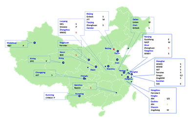
China Wafer Production Capacity Growth Fastest in World
MILPITAS, Calif. – January 7, 2019 – Unwavering in its drive to build a strong, self-sufficient semiconductor supply chain, China plans more new fab projects than any other region in the world from 2017 to 2020, and its expansion of fab capacity recently picked up pace on the strength of new foundry and memory projects from both domestic and foreign companies, according to SEMI’s 2018 China Semiconductor Silicon Wafer Outlook report. China’s installed fab capacity is forecast to grow at a 12 percent CAGR from 2.3 million wafers per month (wpm) in 2015 to 4 million wpm in 2020, faster than all other regions.
Well known for its semiconductor packaging prowess, China in recent years shifted its focus to front-end semiconductor fabs and a few key material markets. In 2018, the region’s surge in fab investment thrust it past Taiwan as the second largest capital equipment market in the world, behind only Korea.
However, China’s semiconductor manufacturing growth faces strong headwinds. Chief among them is the tight supply of silicon wafers over the past two years due in large part to the sector oligopoly’s firm control of global production, with the top five wafer manufacturers accounting for over 90 percent of market revenue. In response, China’s central and local governments has made the development of its domestic silicon wafer supply chain a key initiative, funding multiple silicon wafer manufacturing projects.

According to the 2018 China Semiconductor Silicon Wafer Outlook report, many of China’s domestic silicon suppliers capably provide wafers 150mm in size and smaller. And the while the region lags peers in 200m and 300mm processing technology and capacity, strong domestic demand and favorable policies have fueled progress in 200mm and 300mm silicon manufacturing with some Chinese suppliers having reached key large-diameter manufacturing milestones. However, it will take these new suppliers several years before they can meet capacity and yield requirements of the larger-diameter silicon wafer market. Company plans and announcements indicate that by the end of 2020, total silicon supply capacity in China will reach 1.3 million wpm for 200mm, possibly leading to a slight oversupply, and 750,000 wpm for 300mm.
China’s equipment suppliers, particularly crystal furnace vendors, are also investing in the development of 300mm wafer manufacturing, and domestic tool suppliers have developed most of the necessary tools for wafer manufacturing, except for inspection.
While China’s silicon wafer suppliers continue to lag international peers in manufacturing capabilities, the region’s silicon manufacturing ecosystem is maturing and becoming better integrated. The sector’s growth is driven and accelerated by significant domestic market demand and favorable policies.
About the China Semiconductor Silicon Wafer Outlook
SEMI’s 2018 China Semiconductor Silicon Wafer Outlook is a comprehensive research report with a Microsoft Excel® workbook containing in-depth analysis of China’s silicon wafer manufacturing ecosystem as it relates to the global semiconductor wafer industry. The report covers the latest developments in China’s silicon wafer supply chain, including details on the rise of China’s silicon manufacturing, polysilicon, and silicon wafer-related equipment companies. The report also examines policies, funding and their implications for China’s silicon wafer supply chain.
About SEMI
SEMI® connects over 2,100 member companies and 1.3 million professionals worldwide to advance the technology and business of electronics manufacturing. SEMI members are responsible for the innovations in materials, design, equipment, software, devices, and services that enable smarter, faster, more powerful, and more affordable electronic products. FlexTech, the Fab Owners Alliance (FOA), the MEMS & Sensors Industry Group (MSIG), and Electronic Systems Design Alliance (ESDA), are SEMI Strategic Association Partners, defined communities within SEMI focused on specific technologies. Since 1970, SEMI has built connections that have helped its members prosper, create new markets, and address common industry challenges together. SEMI maintains offices in Bangalore, Berlin, Brussels, Grenoble, Hsinchu, Seoul, Shanghai, Silicon Valley (Milpitas, Calif.), Singapore, Tokyo, and Washington, D.C. For more information, visit www.semi.org
Related Semiconductor IP
- SHA-256 Secure Hash Algorithm IP Core
- EdDSA Curve25519 signature generation engine
- DeWarp IP
- 6-bit, 12 GSPS Flash ADC - GlobalFoundries 22nm
- LunaNet AFS LDPC Encoder and Decoder IP Core
Related News
- Worldwide Silicon Wafer Shipments Increase 7% in Q2 2024, SEMI Reports
- Worldwide Silicon Wafer Shipments Increase 6% in Q3 2024, SEMI Reports
- Worldwide Silicon Wafer Shipments and Revenue Start Recovery in Late 2024, SEMI Reports
- Worldwide Silicon Wafer Shipments Increase 2% Year-on-Year in Q1 2025
Latest News
- AiM Future Partners with Metsakuur Company to Commercialize NPU-Integrated Hardware
- ESD Alliance Reports Electronic System Design Industry Posts $5.5 Billion in Revenue in Q4 2025
- Omnitrx introduces Omni500 Ethernet Evaluation Platform, Built on Comcores Expertise
- Three Misconceptions About the $402B Semiconductor Foundry Industry
- TSMC March 2026 Revenue Report