The MOST Ultimate OTP Technology - AGIC Particle Momentum
April 1, 2019 -- The One-Time-Programming NVM (OTP) is a fundamental memory IP, which is widely used in automotive, aerospace, power management (PMIC), mobile and IoT applications for trimming, security, feature selection and boot codes storage. To choose an ideal OTP solution, designers in semiconductor industry must consider the portability, reliability, and availability on desired process platform with regards to spec. In the past thirty years, the embedded OTP in logic base CMOS processes have been dominated by three different types of technology, Electrical Fuse, Floating Gate OTP, and Anti-Fuse OTP.
Conventional OTP in semiconductor industry
The electrical fuse is widely used in various processes, from 0.5 um to 7 nm and beyond. The basic operating theory of e-Fuse is to use high current to explode either poly fuse or metal fuse with so called “Electron Migration” phenomenon. Although the Fuse type OTP is easy for porting, it unavoidably accompanies with serious issues such as area efficiency, power consumption, and high defect rate, especially in high memory density applications.
The era of embedded floating gate OTP has been on the process nodes with the oxide thickness from 75 Å to 55 Å. With UV erasable feature, the main benefit of this type of OTP is its testability on memory cell. As for the main constraints of floating gate OTP, the oxide thickness and high temperature are two killing factors, which may cause the issue of data retention. Hence, it is rarely to see floating gate OTP solution below 65 nm technology and in highly reliable required applications.
Opposite to floating gate, anti-fuse OTP is by rupturing device’s oxide to perform data writing, which means a thinner oxide thickness is required. In technology node below 65 nm, anti-fuse OTP is almost the main stream for high density OTP solution. Notwithstanding for the advantage of thin oxide, it is suffering from another issue when oxide thickness is too thin – the increasing of gate leakage. From 28 nm node, the gate leakage is way too high and it seriously impacts cell programming yield. Regrettably, the general ways to solve above situation are to add more cell per bit and/or to add more supplements, such as ECC circuit.
The KEY to Flip the World
In modern semiconductor technology, since the oxide thickness remains only several Å, it has to revisit the technology with the aspect of quantum physics, and even steps further into particle physics. Taking electron migration (EM) effect for example, in the past decades, EM effect had been exanimated by its phenomenon. However, it is still mis-used in serval applications with incorrect concept. Even though the fuse type OTP has been designed and merged into various products, it still has difficulty to achieve high programming yield or good area efficiency in high memory density.
Exhilaratingly, in 2017, a scientific team published a paper on Nature Scientific Report and revisited the EM effect with quantum physics, which disclosed the real EM effect should be interaction of electron, thermal and stress migrations. As we witness the end of Moore’s Law, with “REAL TRUETH” of physics, the whole semiconductor industry is just starting to flip.

AGIC Particle Momentum
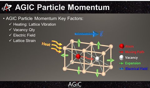
The AGIC Particle Momentum, or we called AGIC momentum, is a progress to control atom movement in semiconductor by controlling the interaction between atom and electron momentum. This is discovered by the team named “AGIC”, by reviewing the semiconductor technology under the fields of quantum physics, particle physics, material science, process, and circuit design. With AGIC momentum, the AGIC team creates the most ultimate solution for OTP, MTP, and even fulfill Qubit for quantum computing and communication for the next future.
About AGICIP Technology:
- A-Fuse, C-Fuse, and D-Fuse
- With NO additional mask Steps in different processes including CMOS, BJT, DRAM, BCD, HV, etc.
- Reliably programmed through a controlled, non-reversible current programmed bits.
- Portable across all Nodes.
- Use the existing standard processes.
- Covering the processes from 350nm to 5nm and beyond.
- Operation temp from -55°C to 175°C and beyond.
- The smallest area of the OTP in the World.
Welcome to visit our web and contact with us for detail presentation and discussion.
AGICIP (www.agicip.com)
Artificial General Intelligence Cosmos IP total solution.
Sales@agicip.com
Related Semiconductor IP
- 6-bit, 12 GSPS Flash ADC - GlobalFoundries 22nm
- LunaNet AFS LDPC Encoder and Decoder IP Core
- ReRAM NVM in DB HiTek 130nm BCD
- UFS 5.0 Host Controller IP
- PDM Receiver/PDM-to-PCM Converter
Related News
- AGIC C-Fuse OTP High-Temperature-Immunity Tailored for AEC-Q100 Grade 0 Applications
- Altera Excalibur Workshops Build Momentum for SOPC Designs
- Momentum builds for open-source processors
- AMBA Interconnect Technology Gains Further Industry Momentum
Latest News
- AGI CPU: Arm’s $100B AI Silicon Tightrope Walk Without Undermining Its Licensees
- EnSilica selected for UK CHERI Adoption Collective
- CHIPS Alliance launches the SV Tools Project for open source development of SystemVerilog/UVM codebases
- Socionext Collaborates with Arm to Advance AI Data Center Infrastructure with Arm Total Design
- EDGEAI to Revolutionize Smart Metering with BrainChip Akida 2 License