transceiver IP
Filter
Compare
967
IP
from
114
vendors
(1
-
10)
-
Wi-Fi 802.11ax + BLE transceiver, 2.4 GHz + PA
- SaberTek offers compact, low-power Wi-Fi 802.11ax transceiver IP with optional integrated BLE and sub-GHz support for multi-protocol IoT platforms
- These solutions combine advanced OFDMA/MIMO capabilities with energy-optimized architectures suitable for consumer, industrial, and wearable applications
-
Ultra-low-power, low-cost sub-GHz 200 MHz – 950 MHz transceiver with PA for WSN
- The IoT and WSN transceiver IP targets long-range, low-power connectivity for dense sensor deployments and industrial networks
- Supporting sub-GHz 802.15.4g, Wi-SUN, and integrated 2.4 GHz operation, these designs provide excellent receiver sensitivity, flexible modulation support, and ultra-low energy consumption
- They are ideal for smart meters, building automation, grid monitoring, and wide-area IoT systems.
-
2.4 GHz 802.11ax + BLE transceiver with integrated sub-GHz path
- SaberTek offers compact, low-power Wi-Fi 802.11ax transceiver IP with optional integrated BLE and sub-GHz support for multi-protocol IoT platforms
- These solutions combine advanced OFDMA/MIMO capabilities with energy-optimized architectures suitable for consumer, industrial, and wearable applications
-
Ultra-low-power, low-cost sub-GHz transceiver for WSN
- The IoT and WSN transceiver IP targets long-range, low-power connectivity for dense sensor deployments and industrial networks
- Supporting sub-GHz 802.15.4g, Wi-SUN, and integrated 2.4 GHz operation, these designs provide excellent receiver sensitivity, flexible modulation support, and ultra-low energy consumption
- They are ideal for smart meters, building automation, grid monitoring, and wide-area IoT systems.
-
LTE Cat-1 bis (200 MHz – 2.5 GHz) wideband transceiver supporting TDD, FD-FDD, and HD-FDD operation—suitable for SDR implementations requiring flexible duplexing architecture.
- The SDR transceiver IP provides wideband, programmable RF front-ends for multi-standard wireless platforms
- These architectures support NB-IoT, Cat-M, custom modem protocols, and future-proof waveform development
- Features include dynamic bandwidth scaling, reconfigurable synthesizers, and digitally assisted calibration for robust performance across process, voltage, temperature, and environmental variations.
-
3.3V CAN Transceiver
- The TS_CAN_3V3_X8 is a 3.3V CAN transceiver, which supports data rates up to 1Mbps and is compatible with ISO 11898-2 compliant CAN transceivers.
- It supports a standby mode with wake up via wake-up pattern.
- The TS_CAN_3V3_X8 provides a symmetrical output signal on CANL/CANH and incorporates slope-control to improve EMI performance.
-
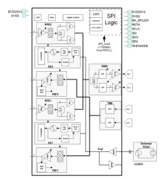
802.15.4G RF Transceiver
- The RF Transceiver (B130RF15P4G) is a dual band (sub-1GHz and 2.4GHz band) integrated transceiver specially designed for smart metering and IEEE 802.15.4g related applications.
-
Sub-1GHz (699MHz-960MHz) fully integrated transceiver
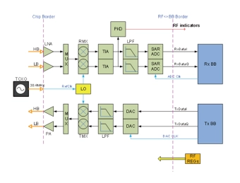
- The B40NLL_NBIOT_TRX is a sub-1GHz (699MHz-960MHz) fully integrated transceiver specially designed for Narrow-band IOT applications.
- The device is comprised of RF frontend, Frac-N frequency synthesizer, LO chains, and analog baseband blocks.
- The receive path (RX) has high dynamic range and sensitivity.
-
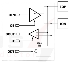
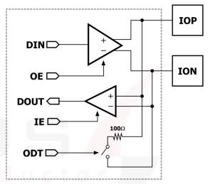
0.9V SLVS Transceiver in TSMC 22nm
- This SLVS I/O Library, implemented in TSMC 22nm with an 11P7M_5X1Z UT-AlRDL metal stack, provides a 0.9V differential transceiver optimized for low-power, high-speed operation.
- Supporting data rates up to 200 Mbps and compliant with JESD8-13 SLVS standards, the library features strong power supply rejection, integrated 100 on-die termination, and robust 2 kV HBM / 500 V CDM ESD protection.
-
1.2V SLVS Transceiver in UMC 110nm
- This library delivers a compact and reliable 1.2V SLVS transceiver solution in UMC 110nm, optimized for high-speed, low-power applications.
- Featuring robust supply and ground noise rejection, 2kV HBM ESD protection, and integrated on die termination, this library provides both transmit and receive paths compliant with JESD8-13 SLVS standards at up to 200 Mbps.