Rambus Controller IP
Filter
Compare
51
IP
from
1
vendors
(1
-
10)
-
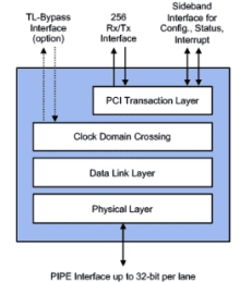
PCIe 3.1 Controller
- Dynamically adjustable application layer frequency down to 8Mhz for increased power savings
- Optional MSI/MSI-X register remapping to memory for reduced gate count when SR-IOV is implemented
- Configurable pipelining enables full speed operation on Intel and Xilinx FPGA, full support for production FPGA designs up to Gen3 x16 with same RTL code
- Ultra-low Transmit and Receive latency (excl. PHY)
- Smart buffer management on receive side (Rx Stream) and transmit side (merged Replay/Transmit buffer) enables lower memory footprint
-
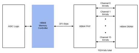
HBM4 Memory Controller
- Supports HBM4 memory devices
- Supports all standard HBM4 channel densities (up to 32 Gb)
- Supports up to 10 Gbps/pin
- Refresh Management (RFM) support
- Maximize memory bandwidth and minimizes latency via Look Ahead command processing
- Integrated Reorder functionality
-
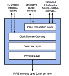
PCIe 7.0 Controller
- Optimized for high-bandwidth efficiency at data rates up to 128 GT/s
- Separate native TX/RX data path separating posted/Non posted/completion traffic
- Handles up to 4 TLPs per cycle
- Advanced PIPE modes and port bifurcation
-
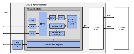
LPDDR5T / LPDDR5X / LPDDR5 Controller
- Support for all LPDDR5T/5X/5 devices
- Bank management logic monitors status of each bank
- Queue-based user interface with reordering scheduler
- Look-ahead activate, precharge, and auto-precharge logic
- Parity protection for all stored control registers
- PHY interface based on DFI 5.1 standard
-
LPDDR4X/4 & LPDDR5T/5X/5 Combo Controller
- Support for all LPDDR4 and LPDDR5 devices
- Bank management logic monitors status of each bank
-
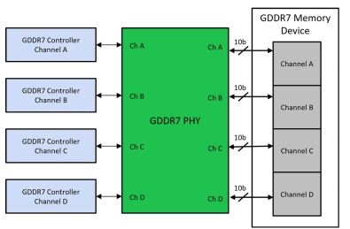
GDDR7 Memory Controller
- Supports up to 40 Gbps per pin operation
- 2.5 GHz CK4 clock
- 1.25 GHz controller clock
- Internal data path 32x memory width (i.e. 256 bits for 8-bit memory)
- Optimized for high efficiency and low latency across a wide range of traffic scenarios (random/sequential, short/long bursts, etc.)
- Optimized command sequence for highest bus utilization including per-bank refresh scheduling: single queue structure handles look-ahead activates/ precharges and read/write ordering for minimal latency
-
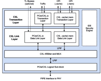
CXL 3.1 Controller
- Ultra-low Transmit and Receive latency
- Internal data path size automatically scales up or down (256, 512 or 1024 bits) based on max. link speed and width for optimal throughput
- Supports backwards compatibility to PCIe 6.1
- Optional MSI/MSI-X register remapping to memory for reduced gate count when SR-IOV is implemented
- Optional QuickBoot mode allows for up to 4x faster link training, cutting system-level simulation time by 20%
- Loopback Mode support at DLL for CXL.mem and CXL.cache protocols
- Merged Replay and Transmit buffer enables lower memory footprint
-
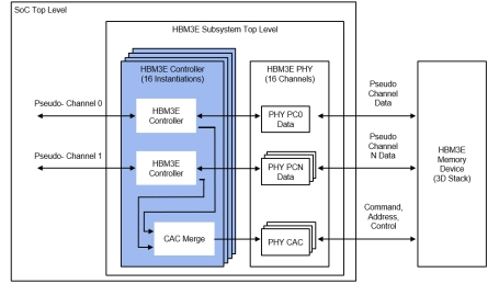
HBM3E/3 Memory Controller
- Supports HBM3E / HBM3 memory devices
- Supports all standard HBM3 channel densities (up to 32 Gb)
- Supports up to 9.6 Gbps/pin (HBM3E) or 8.4 Gbps/pin (HBM3)
- Refresh Management (RFM) support
- Maximizes memory bandwidth and minimizes latency via Look-Ahead command processing
- Integrated Reorder functionality
-
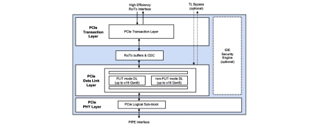
PCIe 6.1 Controller
- Designed to the latest PCI Express 6.1 (64 GT/s), 5.0 (32 GT/s), 4.0 (16 GT/s), 3.1/3.0 (8 GT/s), and PIPE 6.x (8, 16, 32, 64 and 128-bit) specifications
- Supports SerDes Architecture PIPE 10b/20b/40b/80b width
- Supports original PIPE 8b/16b/32b/64b/128b width
- Compliant with PCI-SIG Single-Root I/O Virtualization (SR-IOV) Specification
- Supports multiple virtual channels (VCs) in FLIT and non-FLIT modes
- Supports Endpoint, Root-Port, Dual-mode, Switch port configurations
-
PCIe 2.1 Controller
- Compliant with the PCI Express 2.1/1.1, and PIPE (16- and 32-bit) specifications
- Compliant with PCI-SIG Single-Root I/O Virtualization (SR-IOV) Specification
- Supports Endpoint, Root-Port, Dual-mode, Switch port configurations
- Supports x16, x8, x4, x2, x1 at 5 GT/s and 2.5 GT/s speeds
- Supports AER, ECRC, ECC, MSI, MSI-X, Multi-function, crosslink, and other optional features