DDR Memory IP
Filter
Compare
455
IP
from
64
vendors
(1
-
10)
-
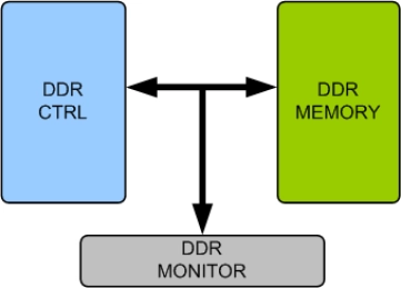
DDR Memory Model
- Supports DDR memory devices from all leading vendors.
- Supports 100% of DDR protocol standard JESD79F.
- Supports all the DDR commands as per the specs.
- Supports all device speeds as per specification.

-
Performance Enhanced version of DDR Enhanced Memory Ctl (uMCTL2) supporting DDR4, DDR3, DDR2, LPDDR4, LPDDR3, and LPDDR2
- Select a complete multi-ported Enhanced Universal DDR Memory Controller offering 1 to 16 host ports, or join a third-party scheduler to a single-port Enhanced Universal Protocol Controller
- Support for JEDEC standard DDR2, DDR3, DDR4, LPDDR/Mobile DDR, LPDDR2, LPDDR3, and LPDDR4 SDRAMs
- Compatible with all Synopsys DDR PHYs (excluding DDR2/DDR PHYs) using DFI-compliant interfaces
-
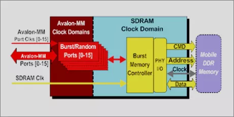
Avalon Mobile DDR Memory Controller
- 200 MHz Cyclone / Stratix memory performance
- Supports all standard Mobile DDR SDRAM devices
- 1 to 16 Avalon® independent local bus port interfaces
- Avalon Pipelined and Burst transfers

-
DO-254 DDR Memory Controller 1.00a
- DDR, DDR2, DDR3, and LPDDR (Mobile DDR) memory standards support
- Up to 800 Mb/s (400 MHz double data rate) performance
- Up to four MCB cores in a single Spartan-6 device
- Configurable dedicated multi-port user interface to FPGA logic
-
PLL general purpose / DDR memory, 50-500Mhz, 4 phases (0/90/180/270)
- 50 to 500Mhz output frequency
- 4 phases 0,90,180 &270 even in bypass mode
- 1P4M layout structure based on 0.18um 1P5M or 1P6M 1.8V logic process
- Single power supply 1.8V±10%, -40/+125°C
-
High Performance DDR 3/2 Memory Controller IP
- Supports DDR3/DDR2 SDRAM
- 16 bits width DDR2/DDR3 SDRAM Interface
- Memory Clock up to 462MHz, DFI Clock up to 462MHz
- Support DDR2 667/800/1066 and DDR3 667/800/1066/1333/1600/1866
-
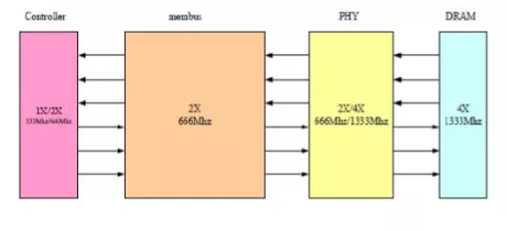
DDR 4/3 Memory Controller IP - 2400MHz
- Support s DDR 4 /DDR3 SDRAM
- 16 bit s width , Single Channel DDR 4 /DDR3 SDRAM Interface .
- 16 bits for per channel, could support 2 x8 bits DDR3, but could not support 2 x8 bits DDR4.
- Memory Clock up to 6 66 MHz, DFI Clock up to 666 MHz .

-
DDR Memory Controller IP for low power and high reliability
- Supports DDR protocol standard JESD79F Specification.
- Compliant with DFI-version 2.0 or higher Specification.
- Supports all the DDR commands as per the specs. Supports up to 16 AXI ports with data width upto 512 bits.
- Supports controllable outstanding transactions for AXI write and read channels
-
SDRAM DDR Controller
- Dolphin Technology offers high performance DDR4/3/2 SDRAM and LPDDR5/4x/4/3/2 SDRAM Memory Controller IP across a broad range of process technologies.
-
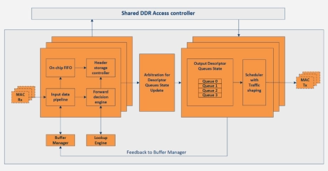
Deep Buffering Memory 1G Ethernet Switch
- The 1G deep buffering memory Ethernet Switch is an advanced Ethernet switching IP that supports buffering large amounts of data in external RAM.
- The non-blocking Ethernet switch IP core enables fine-grained traffic differentiation for rich implementations of packet prioritization, enabling per port and per queue shaping on egress ports.
