DDR Combo PHY IP
Filter
Compare
20
IP
from
8
vendors
(1
-
10)
-
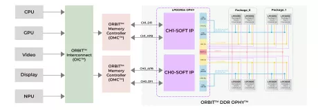
DDR and LPDDR Combo PHY
- Supports multiple combinations of DDR/LPDDR interfaces
- Compliant with JEDEC DDR and LPDDR standards
- Supports all auto calibrations
- Industry leading area and power
-
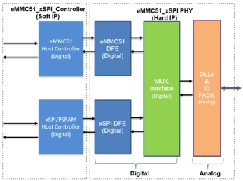
xSPI + eMMC Combo PHY IP
- This IP integrates both xSPI (Expanded Serial Peripheral Interface) and eMMC 5.1 PHY (Physical Layer) into a single unified solution, enabling support for two distinct memory protocols within the same IP.
- By combining the PHY layers for both interfaces, the design simplifies system integration, reduces area and pin count, and enhances design flexibility for SoCs that require both boot and high-speed storage functionality.
-
LPDDR5X/5/4X/4 combo PHY at 12nm
- Compliant with JEDEC JESD209-5C for LPDDR5x/5/4x/4 with PHY standards
- Delivering up to 8533Mbps
- DFI 5.1 specification PHY Interface Compliant
- Support up to 4 ranks
- Multiple frequency states

-
LPDDR5X/5/4X/4 combo PHY at Samsung SF5A
- Compliant for JEDEC standards for LPDDR5X/5/4X/4 with PHY standards
- DFI 5.1 specification PHY Interface Compliant
- Support up to 4 ranks
- x16 and x32 channel support

-
LPDDR5X/5/4X/4 combo PHY at 7nm
- Compliant with JEDEC JESD209-5B for LPDDR5X/5/4X/4 with PHY standards
- Delivering up to 8533Mbps
- DFI 5.1 specification PHY Interface Compliant
- Support up to 4 ranks
-
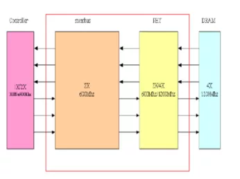
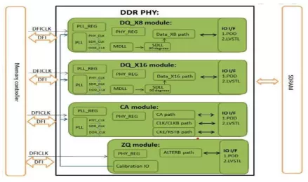
DDR PHY
- Dolphin's hardened DDR4/3/2 SDRAM PHY and LPDDR5/4x/4/3/2 SDRAM PHY IP is a silicon-proven, Combo PHY supporting speeds up to 4266 Mbps.
- It is fully compliant with the DFI 4.0 specification, and features include slew rate control, per-bit de-skew, gate training, read and write leveling and built-in self test (BIST).
- In addition, our PHY IP is optimized to provide a complete solution when combined with Dolphin's DDRx and LPDDRx SDRAM Memory Controller IP.
-
DDR5/DDR4/LPDDR5 Combo PHY IP - 4800Mbps (Silicon Proven in TSMC 12FFC)
- Supported DRAM type: DDR5/DDR4/LPDDR5
- Maximum controller clock frequency of 675MHz resulting in maximum DRAM data rate of 5400MT/s for DDR5
- Maximum controller clock frequency of 400MHz resulting in maximum DRAM data rate of 3200MT/s for DDR4
- Maximum controller clock frequency of 600MHz resulting in maximum DRAM data rate of 4800MT/s for LPDDR5?
-
LPDDR5/4x/4 combo PHY on 14nm, 12nm
- Compliant with JEDEC standards for LPDDR5/4x/4 with PHY standards
- DFI 5.0 Interface Compliant
- Supports 1,2, or 4 ranks
- Multiple frequency states

-
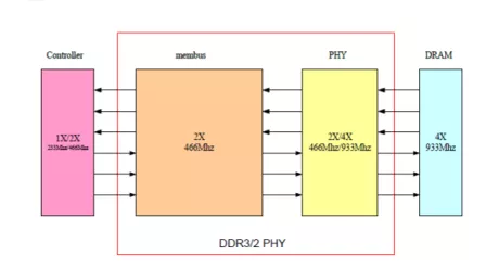
DDR3/ DDR2 Combo PHY IP - 1866Mbps (Silicon Proven in UMC 40LP)
- Supports DDR3/DDR2 SDRAM
- DDR3 JEDEC standard 1.5v I/O (SSTL_15- compatible)
- DDR2 JEDEC standard 1.8v I/O (SSTL_18- compatible)
- 16 bits width, Single Channel DDR3/DDR2 SDRAM Interface.
-
DDR4/ DDR3 Combo PHY IP - 2400Mbps (Silicon Proven in UMC 28HPC+)
- Supports DDR4/DDR3 SDRAM
- DDR4 JEDEC standard 1.2v I/O (POD_12 I/O)
- DDR3 JEDEC standard 1.5v I/O (SSTL_15-compatible)
- 16 bits width, Single Channel DDR4/DDR3 SDRAM Interface.