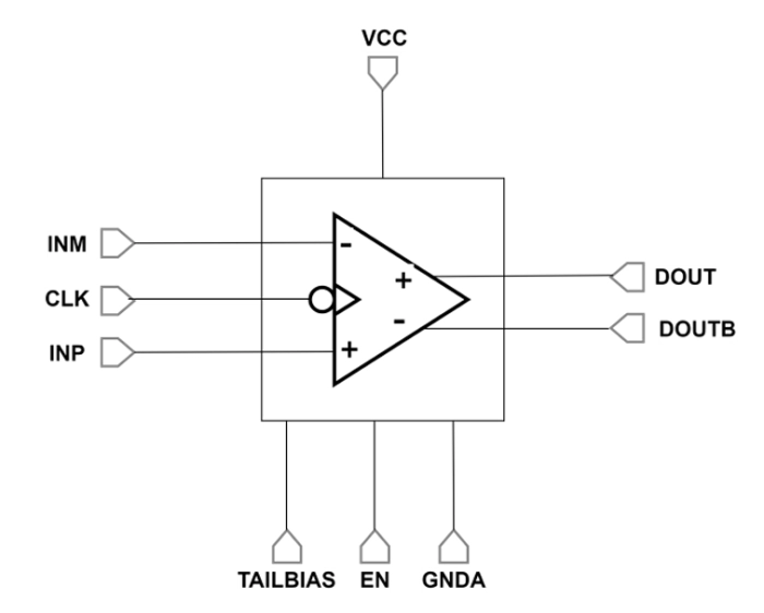
A high-speed voltage clocked comparator with rail- to-rail outputs and no hysteresis. The typical propagation delay is 19ns while applying a differential input signal of 1mV over the offset voltage. The comparator operates with a supply voltage of 3.3V typical (VCC). The valid input voltage range is between 0.6V up to VCC. The comparator achieves an input offset voltage of ±1.04mV (3-sigma value). The circuit features an Enable signal turning on/off the comparator.
The comparator uses positive feedback (latch) to increase the comparison speed; thus, its operation consists of a reset phase and a regeneration (comparison) phase, which are controlled by the input clock (CLK). When CLK is ‘High’, the comparator is in the reset phase, and when it is ‘Low’, the comparator compares the voltages at INM and INP inputs and produces a 0 or VCC-level digital output voltage at the outputs DOUT and DOUTB. The CLK frequency is 2MHz. An output latch ensures that DOUT and DOUTB retain their previous values during reset phase.
The comparator features zero static current and low kickback noise. It requires a bias current of 89uA supplied from an external biasing circuit via the TAILBIAS input.